
Circuit Diagram
Index 1168
3_3_4_DIGIT_DVM_FOUR_DECADE_±04_V_±4_V_±40_V_AND±400_V_FULL_SCALE
Published:2009/7/1 21:21:00 Author:May

View full Circuit Diagram | Comments | Reading(896)
SHUTTER_SPEED_TESTER
Published:2009/7/1 21:20:00 Author:May

Circuit NotesThe soiar cell is connected across the input of the FET (fleld-effect transistor), Q1, so that it will produce positive dc voltage to the gate when activated by light shining through the open shutter, decreasing the negative gate-source bias already established by the source resistor, and causes an increase in drain current. The drain voltage goes more negative which causes a decrease in Q2's base current. Q2's collector current decreases, and its collector voltage becomes more positive. There is an amplified positive-going voltage output at the collector, and it's applied directly to the oscilloscope's vertical input, producing a waveform that is displaced vertically whenever light strikes the cell. (View)
View full Circuit Diagram | Comments | Reading(1009)
Electronic_thermometer
Published:2009/7/24 3:11:00 Author:Jessie

Fig. 13-42 This very simple circuit is an electronic thermometer using an inexpensive silicon transistor (2N2222) as the temperature sensor or probe. The circuit provides better than 1℃ accuracy over a 100℃ range. An LM113 diode regulates the input voltage to 1.2 V. The 1.2 \/ is applied through R2 to set the operating current of the temperature-sensing 2N2222. R4 biases the amplifier output for zero output at 0℃, while feedback resistor R5 calibrates the output scale factor to 100 mV/℃. Once the output is zeroed, the scale factor does not change the zero. National Semiconductor Linear Applications Handbook 1991, p 171. (View)
View full Circuit Diagram | Comments | Reading(0)
Single_cell_inverting_20_dB_amplifier
Published:2009/7/24 3:11:00 Author:Jessie

Total power consumption for this circuit is about 675 nA. The output voltage swing is 300 mVPP, with a 20-kΩ load. (View)
View full Circuit Diagram | Comments | Reading(625)
Transformer_driver_for_isolated_RS485_interface
Published:2009/7/24 3:11:00 Author:Jessie


Figures 3-66, 3-67, and 3-68 show the block diagram, pin descriptions, and test circuit for the MAX253. Figures 3-69 through 3-72 show recommended component suppliers. This IC is a monolithic oscillator/driver specifically designed to provide isolated power for an isolated RS485 or RS-232 data interface. The IC drives a center-tapped transformer primary from a 5-V or 3.3-V supply. The secondary can be wound to provide any isolated voltage needed at power levels up to 1 W. The oscillator runs at double the output frequency, driving a toggle flip-flop to ensure a 50% duty cycle to each of the switches. The current is 0.4 μA in shutdown. Figures 3-73 through 3-82 show typical circuits for a variety of applications,MAXIM NEW RELEASES DATA BOOK,1995,P. -125,2-136,2-127,2-128,2-129,2-130,2-131,2-132,2-133,2-134,2-135.
(View)
View full Circuit Diagram | Comments | Reading(2562)
5_V_prese_output-efficiency_controller
Published:2009/7/24 3:11:00 Author:Jessie

Figure 7-67 shows a MAX770 connected to provide 5-V output at 1 A with a 3-Vinput Figure 7-68 shows component suppliers. MAXIM NEW RELEASES DATA Book 1995 P. 4-150.4-149. (View)
View full Circuit Diagram | Comments | Reading(599)
STEREO_MULTIPLEX_A_F_AMPLIFIER
Published:2009/7/24 3:10:00 Author:Jessie
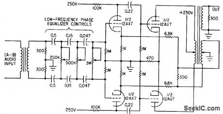
Provides low-frequency phase equalization for the A-B channel, using variable R.C high-pass filter sections that can be adjusted for cutoff between 5 and 25 cps.-Modifying an F-M Transmitter for Compatible Stereo Multiplex, Electronics, 34:28, p 60-62. (View)
View full Circuit Diagram | Comments | Reading(1292)
5_DIGIT_LED_REAL_TIME
Published:2009/7/1 21:20:00 Author:May
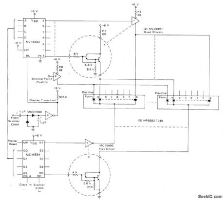
Circuit providesstrobing of LEDs so peak current and light output are greater for same average current Peak fotward current for display is about 40 mA. All Iike anode segments of common-cathode displays are driven by emitter outputs of MC75491 quad drivers.-A. Pshaenich, Interface Considerations for Numeric Display Systems, Motorola, Phoenix, AZ, 1975, AN-741, p 13. (View)
View full Circuit Diagram | Comments | Reading(604)
5_MHz_PHASE_ENCODED_DATA_READ_CIRCUITRY
Published:2009/7/1 21:18:00 Author:May
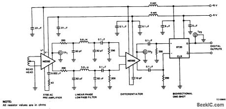
Readback data is applied directly to the input of the first NE592. This amplifier functions as a wide-band ac coupled amplifier with a gain of 100. By direct coupling of the readback head to the amplifier, no matched terminating resistors are required and the excellent common-mode rejection ratio of the amplifier is preserved. The dc components are also rejected because the NE592 has no gain at dc due to the capacitance across the gain select terminals. The output of the first stage amplifier is routed to a linear phase shift low-pass filter, with a characteristic impedance of 200 ohms. The second NE592 is utilized as a low noise differentiator/amplifier stage. The output of the differentiator/amplifier is connected to the 8720 bidirectional monostable unit to provide the proper pulses at the zero-crossing points of the differentiator. (View)
View full Circuit Diagram | Comments | Reading(555)
V_F_CONVERSION,NEGATIVE_INPUT_VOLTAGE
Published:2009/7/1 21:18:00 Author:May

View full Circuit Diagram | Comments | Reading(471)
PULSE_COINCIDENCE_DETECTOR
Published:2009/7/1 21:18:00 Author:May

Unless inputs A and B (2- to 3-V amplitude) occur simultaneously no voltage exists across RL. Less than 1 microsecond overlap is sufficient to trigger the scs. Coincidence of negative inputs is detected with gates GA instead of GC by using the scs in a complementary SCR configuration. (View)
View full Circuit Diagram | Comments | Reading(0)
327_Hz_HIGH_PASS
Published:2009/7/1 21:17:00 Author:May

Developed to make third harmonic of 130.81 Hz (C3 note) minimum of 30 dB stronger than fundamental, to give sawtooth output for use in electronic music system. Design uses third-order filter with 3-dB dips in response. Opamp can be 741.-D. Lancaster, Active-Filter Cookbook, Howard W. Sams, Indianapolis, IN. 1975. p 192. (View)
View full Circuit Diagram | Comments | Reading(526)
AUTO_ADVANCE_PROJECTOR
Published:2009/7/1 21:17:00 Author:May
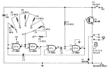
Circuit Notes
The circuit is built around a 4001 quad two-input N0R gate, it provides switch selectable auto-advance times of 5,10, 15, 20, 25 or 30 seconds through the remote-control socket of your projector. U1a and U1b form an astable multivibrator, with its operating frequency dependent on the number of timing resistors switched into the circuit via S2. The frequency is about one cycle for every five seconds with a single timing resistor, one every ten seconds with two resistors, etc., providing six switched time intervals. The output of the astable at pin 4 of U1b is fed to the input of a monostable multiibrator, consisting of the second pair of gates, U1c and U1d. R7 and C3 are the timing components; they set the length of the (positive) output pulse of the monostable at a little more than half a second. The monostable is triggered by each positive-going input it receives from the astable. The output from the monostable therefore, consists of a series of short pulses, the interval between the pulses being controlled using S2.The output of the monostable (at pin 11) controls a relay by way of Q1, which is configured as an emitter-follower buffer stage. The projector is controlled via the normally-open contacts of relay K1. When the output of the monostable goes positive, the relay contacts close, triggering the slide-change mechanism of the projector. The monostable assures that the power to the relay is applied only briefly by the timer, so that multiple operation of the projector is avoided. (View)
View full Circuit Diagram | Comments | Reading(1190)
DIFFERENTIAL_HOLD
Published:2009/7/1 21:17:00 Author:May
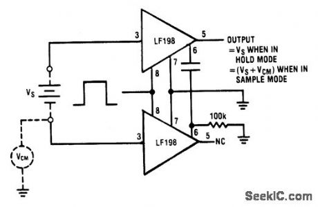
View full Circuit Diagram | Comments | Reading(0)
ULTRAPRECISION_V_F_CONVERTER
Published:2009/7/1 21:17:00 Author:May

The circuit is capable of better than 0.02% error and 0.003% nonlinearity for a ±20℃ range about room temperature. (View)
View full Circuit Diagram | Comments | Reading(0)
TWO_MESSAGES_WITH_NlXlES
Published:2009/7/1 21:16:00 Author:May
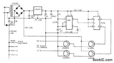
Circuit flashes two messages altemately on same Burroughs giant Nixie B7971 display. Lighted segments needed on individual Nixies to form desired wording are divided into three strings. Segments A are common to both sets of letters and numbers. Segments B are those required with A segments to form first message. Segments C are those required with A segments to form second message. Changeover from segments B to C is done with switching transistors controlled by 555 timer and 7476 or 7473 flipflop. Decimal or other punctuation is formed with NE2 ndon and 100K resistor wired in series between pin 13 of a Nixie and B or C. Article gives construction details.-J. Grimes, Put Your Name in Lights, 73 Magazine, Nov. 1976, p 60-61. (View)
View full Circuit Diagram | Comments | Reading(723)
TWO_WIRE_TONE_ENCODER
Published:2009/7/1 21:16:00 Author:May
View full Circuit Diagram | Comments | Reading(529)
4_CHANNEL_COMMUTATOR
Published:2009/7/1 21:16:00 Author:May
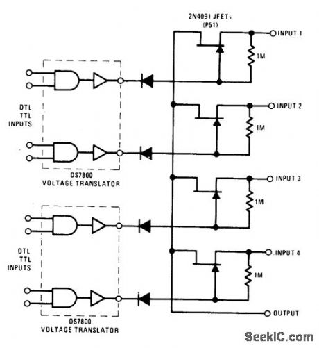
This 4-channel commutator used the 2N4091 to achieve low channel on resistance (<30 ohm) and low off current leakage. The DS7800 voltage translator is a monolithic device that provides from 10 V to -20 V gate drive to the JFETs while at the same time providing DTL/TTL logic compatibility. (View)
View full Circuit Diagram | Comments | Reading(918)
FREQUENCY_LIMIT_DETECTOR
Published:2009/7/1 21:15:00 Author:May

Simple frequency limit detectors providing a GO/NO-GO output for use with varying amplitude input signals may be conveniently implemented with the ICL8211/8212. In the application shown, the first ICL8212 is used as a zero-crossing detector. The output circuit consisting of R3, R4 and C2 results in a slow output positive ramp. The negative range is much faster than the positive range. R5 and Rg provide hysteresis so that under all circumstances the second ICL8212 is turned on for sufficient time to discharge C3.The time constant of R7C3 is much greater than R4C2. Depending upon the desired output polarities for low and high input frequencies, either an ICL8211 or an ICL8212 may be used as the output driver.The circuit is sensitive to supply voltage variations and should be used with a stabilized power supply. At very low frequencies the output will switch at the input frequency. (View)
View full Circuit Diagram | Comments | Reading(0)
GUITAR_AND_BASS_TUNER
Published:2009/7/1 21:14:00 Author:May
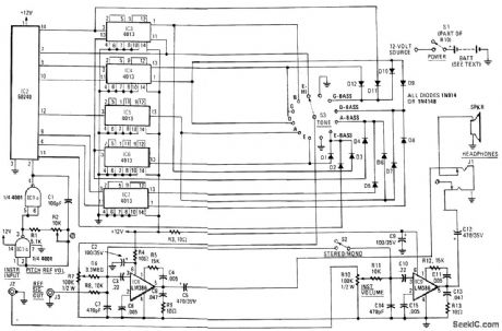
The heart of the circuit is IC2, a 50240 top-octave generator. That device uses a single input-frequency to generate all twelve notes of the musical scale. The input signal is provided by IC1, a 4001 quad 2-input NOR gate. Two sections of that IC are used to form an oscillator that runs at approximately 2 MHz. The frequency can be adjusted by trimmer potentiometer R2. Dual D flip-flops, IC3-IC7, are used as frequency dividers. They divide down the upper-octave frequencies from IC2, thus generating the lower-frequency notes required for the pitch references. The chords for the bass pitchreferences are composed of three notes each. Those notes are taken from various outputs of IC2-IC7 through isolation diodes D1-D12. A1 signals are routed to the TONE switch, S3. The wiper arm of that switch is connected through R7 to the input of audio power-amplifier IC8, an LM386. The resistor acts as a volume control for the pitch reference.Another LM386, IC9, serves as an amplifier for the instrument being tuned, with R10 acting as its volume control. The outputs of IC8 and IC9 are coupled, through C5 and C12 respectively, to the headphone jack, J1. Switch S2 STEREO/MONO is used to mix the reference and instrument signals at IC9 for mono operation. Power is supplied by eight AA cells connected in series. (View)
View full Circuit Diagram | Comments | Reading(1639)
| Pages:1168/2234 At 2011611162116311641165116611671168116911701171117211731174117511761177117811791180Under 20 |
Circuit Categories
power supply circuit
Amplifier Circuit
Basic Circuit
LED and Light Circuit
Sensor Circuit
Signal Processing
Electrical Equipment Circuit
Control Circuit
Remote Control Circuit
A/D-D/A Converter Circuit
Audio Circuit
Measuring and Test Circuit
Communication Circuit
Computer-Related Circuit
555 Circuit
Automotive Circuit
Repairing Circuit