
Circuit Diagram
Index 1170
TWO_DECADE_HIGH_FREQUENCY_VCO
Published:2009/7/1 21:02:00 Author:May

View full Circuit Diagram | Comments | Reading(762)
PUSH_ON_PUSH_OFF_ELECTRONIC_SWITCH
Published:2009/7/1 21:01:00 Author:May

Transistors Q1 and Q2 make up the flip-flop while Q3 drives a reed relay. When powe is first applied to the circuit, Q1 and Q3 are conducting and Q2 is cut off.Momentarily closing S1 causes the flip-flop to switch states-Q1 cuts off and Q2 conducts.When Q2 is conducting, its collector drops to around 0.6 volt. That prevents base current from flowing into Q3 so it is cut off, de-energizing relay K1. The flip-flop changes state every time S1 is pressed. Capacitors C1 and C2 ensure that Q1 is always the transistor that turns on when power is first applied to the circuit. When power is first applied to the basic flip-flop, the initial status is random-Q1 and Q2 both try to conduct and, usually, the transistor with the higher gain will take control, reaching full conduction and cutting off the other one. However, differences in the values of the collector and coupling resistors will also influence the initial state at power-on. With C2 in the circuit, it and R4 form an R-C network that slightly delays the rise in Q2's base voltage. That glves Q1 sufficient time to reach saturation and thus take control. (View)
View full Circuit Diagram | Comments | Reading(6271)
LVDT_signal_conditioner_mechanical_position
Published:2009/7/24 3:23:00 Author:Jessie
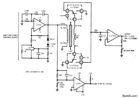
Fig. 14-2 This circuit converts mechanical position (±2.5 mm) into a corresponding output voltage (±2.5 V) using an LVDT (linear variable differential transformer) and an LTC1043 switched-capacitor IC. An LVDT is a transformer with a mechanically actuated core. The primary is driven by a stable sine wave. Two secondaries are connected in opposed phase. When the core is positioned in the magnetic center of the transformer, the secondary outputs cancel and there is no output. Moving the core away from the center position unbalances the flux ratio between the secondaries and develops an output. The output is positive when the core moves in one direction and negative when the core moves in the opposite direction. The circuit output thus indicates how far the core is from center and on which side. To calibrate, center the LVDT core in the transformer and adjust the phase trim for 0-V output. Next, move the core to either extreme position and set the gain trim for 2.50-V output (either positive or negative, depending on which direction the core is positioned). Linear Technology Linear Applications Handbook, 1990. p. AN3-9. (View)
View full Circuit Diagram | Comments | Reading(5121)
THREE_DECADES_VCO
Published:2009/7/1 21:01:00 Author:May

View full Circuit Diagram | Comments | Reading(700)
STEREO_AMPLIFIER_POWER_SUPPLY
Published:2009/7/24 3:23:00 Author:Jessie
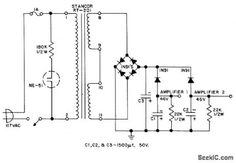
Diode decoupling provides 80 db of separation between two stereo amplifier channels. Designed for use with 10-W power amplifiers.- Transistor Manual, Seventh Edition, General Electric Co., 1964, p 261. (View)
View full Circuit Diagram | Comments | Reading(690)
SPEED_SWITCH
Published:2009/7/1 21:01:00 Author:May

National LM2907 tachometer IC is used as switch to energize load when input frequency exceeds value corresponding to predetermined speed limit. Automotive applications include use as overspeed warning that activates audible and/or visual indicator when auto speed exceeds legal limit or other desiredvalue. Another application is increasing intensity of auto or taxi horn above predetermined speed such as 45 mph. Input is variable-reluctance magnetic pickup positioned against teeth of gear wheel; in typical setup, pickup output is 16.6 Hz at 60 mph. Values shown for comparator-controlling components R1 and C1 (below IC) give switching operation at about 16.6 Hz at input. Report gives design procedure for other frequencies.- Linear Applications, Vol. 2, National Semiconductor, Santa Clara, CA, 1976, AN-162, p 8. (View)
View full Circuit Diagram | Comments | Reading(0)
Micropower_high_input_impedance_amplifier
Published:2009/7/24 3:22:00 Author:Jessie

As shown by the table, standby power is 90 μW, with a 20-MΩ input impedance. (View)
View full Circuit Diagram | Comments | Reading(644)
24_V_preset_output_controller
Published:2009/7/24 3:22:00 Author:Jessie

Figure 7-73 shows a MAX773 connected to provide 24-V output at 30 mA, with a 5-V input. See Fig. 7-69 for component suppliers. MAXIM NEW RELEASES DATA Book, 1995, P. 4-151. (View)
View full Circuit Diagram | Comments | Reading(632)
LEVEL_DETECTOR
Published:2009/7/1 21:00:00 Author:May

By using the ICL7612 in these applications, the circuits will follow rail to rail inputs. (View)
View full Circuit Diagram | Comments | Reading(0)
500_MHz_100_W_push_pull_amplifier
Published:2009/7/24 3:22:00 Author:Jessie
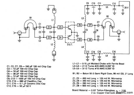
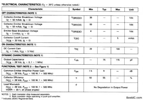
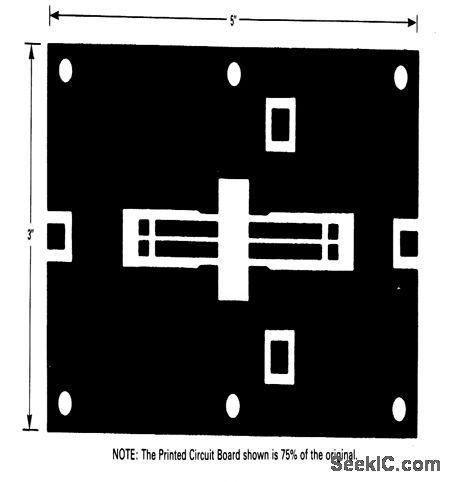
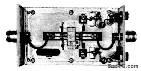
The electrical characteristics for the 2N6986(push-pull transistor)shown in this circuit are gilven in Fig.2-42B Figures 2-42C and 2-42D show the photomaster, and parts location, respectively. Those not familiar with microstrip techniques(for Z1 through Z8)should read the many Motorola publications, such as AN548A and AN555.
(View)
View full Circuit Diagram | Comments | Reading(703)
SIMPLE_VOLTAGE_CONTROLLED_OSCILLATOR
Published:2009/7/1 21:00:00 Author:May

With the component values shown, the oscillator has a frequency of 8 kHz. When an input signal is applied to the base of Q1 the current flowing through Q1 is varied, thus varying the time required to charge C1. Due to the phase inversion in Q1 the direction of output frequency change is 180 degrees out of phase with the input signal. The output may be used to trigger a bistable flip-flop. (View)
View full Circuit Diagram | Comments | Reading(937)
Low_porter_RS_485_RS_422_transceivers
Published:2009/7/24 3:16:00 Author:Jessie


Figure 3-83 shows the typical application circuit and pin configurations for the MAX481/83/85/87. Figures 3-84, 3-85, and 3-86 show the pin functions. Figure 3-87 is the selection table. Figures 3-88 and 3-89 show typical application circuits and pin configurations for the MAX488 through MAX491. Figure 3-90 shows the 1NlAX481/83/85/87 in a typical RS-485 network. Figure 3-91 shows the MAX488 through MAX491 connected in a full-duplex RS485 network. Figure 3-92 shows the MAX488 through MAX491 connected as a line repeater. MAXIM NEW RELEASE DATA BOOK, 1995, P. 2-t59, 2-165, 2-166, 2-167, 2-168, 2-171, 2-172. (View)
View full Circuit Diagram | Comments | Reading(2019)
VOLTAGE_CONTROLLED_OSCILLATOR
Published:2009/7/1 20:59:00 Author:May

The VCO circuit, which has a nonlinear transfer characteristic, will operate satisfac-torily up to 200 kHz. The VCO input range is effective from1/3 VCC to VCC - 2 V, with the highest control voltage producing the lowest output frequency. (View)
View full Circuit Diagram | Comments | Reading(229)
PRECISION_VOLTAGE_CONTROLLED_OSCILLATOR
Published:2009/7/1 20:58:00 Author:May

RC 4151 precision voltage-to-frequency converter generates a pulse train output linearly proportional to the input voltage. (View)
View full Circuit Diagram | Comments | Reading(2228)
0_to_100℃_025℃_accurctte_thermistor_based_temperature_measurement
Published:2009/7/24 3:16:00 Author:Jessie
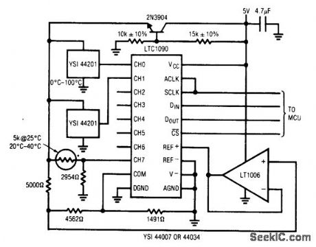
Fig. 13-45 This circuit is an 8-channel, 0 to 100℃, temperature-measurement system, with 0.1℃ resolution. The YSI thermilinear components are measured directly. Accuracy is limited by the sensor repeatability and precision resistors to 0.25℃. Linear Technology Linear Applications Handbook 1990 p DN5-2.
(View)
View full Circuit Diagram | Comments | Reading(482)
STEREO_MULTIPLEX_OSCILLATOR
Published:2009/7/24 3:16:00 Author:Jessie
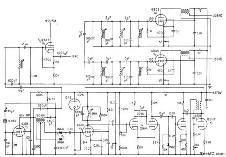
Output of 19-kc crystal oscillator is amplified by V2 for pilot subcarrier. Same frequency is doubled by D1-D2, amplified by V3, and shaped by monostable mvbr V4 to provide trigger pulses. for blocking oscillator VS, from which fifth and sixth harmonics (190 and 228 kc) are taken and amplified by V6 and V7 for use as carrier signals.-Modifying an F-M Transmitter for Compatible Stereo Multiplex, Electronics, 34:28, p 60-62. (View)
View full Circuit Diagram | Comments | Reading(779)
PEAK_DETECTOR
Published:2009/7/1 20:57:00 Author:May


Circuits are easily implemented using the CA3130 BiMOS op amp. For large-signal inputs the bandwidth of the peak-negative circuit is less than that of the peak-positive circuit. The second stage of the CA3130 limits bandwidth in this case. (View)
View full Circuit Diagram | Comments | Reading(3023)
MUSICAL_BELLS
Published:2009/7/1 20:57:00 Author:May

Opamp connected as active filter simulates attack followed by gradual decay as produced when bell or tuning fork is struck. Filter portion of circuit uses twin-T network adjusted so active filter breaks into oscillation when slight external disturbance is intro-duced by closing S1 momentarily. Circuit feeds external audio amplifier and loudspeaker for converting ringing frequency into audible sound. Set R3 just below oscillation point. R1and R2 can be adjusted to give sounds of other musical instruments, such as drums, bamboo, and triangles.-F. M. Mims, Electronic Music Projects, Vol. 1, Radio Shack, Fort Worth, TX, 1977, 2nd Ed., p 71-80. (View)
View full Circuit Diagram | Comments | Reading(1335)
MODEL_ROCKET_LAUNCHER
Published:2009/7/1 20:56:00 Author:May
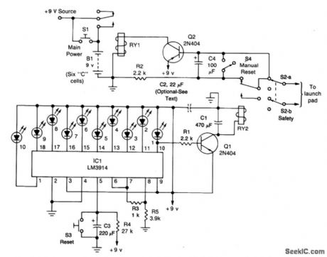
The circuit consists of the launch timer itself and an automatic-off timer. When power is applied to that IC, the countdown LED's sequence is on until they are all lit. When the last one LED1, is fully lit, transistor Q1 saturates, energizing RY2. When that happens, a circuit between the lantern battery at the launch pad and the nickel-chromium wire is completed; the wire heats up as before, and the rocket is launched. Resistor R4 and capacitor C3 determine the countdown timing; with the values shown it should be approximately 10 seconds. Resistors R3 and R5 set the LED brightness. Safety is of the utmost importance. That's the purpose of the second half of the circuit. When RY2 opens, the current flow to Q2 is disrupted. But, because of the presence of R2 and C4, the transistor remains saturated for about 3 seconds. After that, however, the transistor stops conducting and RY1 is de-energized. That cuts off the power to the rest of the circuit, and RY2 de-energizes again, breaking the circuit to the launch pad. Switch S3 is used to reset the countdown. Once that is done, pressing S1 starts the launch sequence; the rest is automatic. Switch S4 is used to latch RY1 manually if needed. (View)
View full Circuit Diagram | Comments | Reading(1193)
6_DIGIT_FLUORESCENT_TRIODES
Published:2009/7/1 20:56:00 Author:May
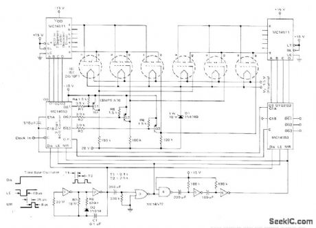
Uses two sets of cascaded counters and decoders with series switching of positive voltage to anode with MC14511 ICs. Digit scanning is accomplished by turning on grid control transistors Q1-Q3 with negative-going digit select outputs of one MC14553, Timing for counters is derived from MC14572 logic elements, with disable pulse obtained from two astable MVBRs. Display digits can be packaged individually or in single envelope.-A. Pshaenich, Interface Considerations for Numeric Display Systems, Motorola, Phoenix, AZ, 1975, AN-741, p 9. (View)
View full Circuit Diagram | Comments | Reading(1038)
| Pages:1170/2234 At 2011611162116311641165116611671168116911701171117211731174117511761177117811791180Under 20 |
Circuit Categories
power supply circuit
Amplifier Circuit
Basic Circuit
LED and Light Circuit
Sensor Circuit
Signal Processing
Electrical Equipment Circuit
Control Circuit
Remote Control Circuit
A/D-D/A Converter Circuit
Audio Circuit
Measuring and Test Circuit
Communication Circuit
Computer-Related Circuit
555 Circuit
Automotive Circuit
Repairing Circuit