
Circuit Diagram
Index 1171
SQUIB_FIRING_CIRCUIT_Ⅱ
Published:2009/7/1 20:54:00 Author:May
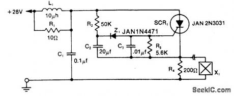
The LRC input network limits the anode dvidt to a safe value-below 30V/μs. R1 provides critical damping to prevent voltage overshoot. While a simple RC filter section could be used, the high current required by the squib would dictate a small value of resistance and a much larger capacitor. Resistor R3 provides dc bias stabilization, while C3 provides stiff gate bias during the transient interval when anode voltage is applied.The SCR is fired one second after arming by means of the simple R2C2Z1 time delay network. R4 provides a load for the SCR for testing the circuit with the squib disconnected-limiting the current to a level well within the continuous rating of the SCR.The circuit can be reset by opening the +28 V supply and then re-arming. (View)
View full Circuit Diagram | Comments | Reading(646)
SQUIB_FIRING_CIRCUIT_Ⅰ
Published:2009/7/1 20:53:00 Author:May
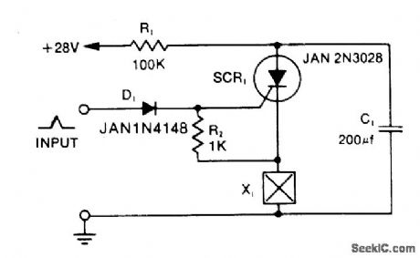
Capacitor C1 is charged to + 28V through R1 and stores energy for firing the squib. A positive pulse of 1mA applied to the gate of SCR1 will cause it to conduct, discharging C1 into the squib load X1. With the load in the cathode circuit, the cathode rises immediately to +28 V as soon as the SCR is triggered on.Diode D1 decouples the gate from the gate trigger source, allowing the gate to rise in potential along with the cathode so that the negative gate-to-cathode voltage rating is not exceeded. This circuit will reset itself after test firing, since the available current through RI is less than the holding current of the SCR. After C1 has been discharged, the SCR automatically turns off-allowing C1 to recharge. (View)
View full Circuit Diagram | Comments | Reading(685)
ZERO_SUPPRESSION
Published:2009/7/1 20:52:00 Author:May

Simple CMOS circuit using MC14011 quad two-input NAND gate and MC14558 IC provides zero suppression for multiplexed displays in which scanning is left to right for leading-zero suppression and right to left for trailing zeros. Article covers operation of circuit.-J. J. Roy, Eliminate Excess Zeros in Multiplexed Displays, EDN Magazine, Sept. 5, 1975, p 77. (View)
View full Circuit Diagram | Comments | Reading(1737)
AUTOMATIC_REMOTE_RHYTHM_CONTROL
Published:2009/7/1 20:52:00 Author:May
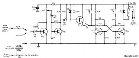
When added to electronic organ,circuitis activated by audio signal from lower manual or pedal, to initiate start of rhythm accompaniment. High-impedance input conhection through 100K ts made to toneshaper output, and transformer connection is used with electromechanical Hammond organ. Transistorand diode types are not critical. If S1 is closed, current passes through to Tr5 and triggers bistable that pulls in relay,S2 and S3 are usedfor manualstart and stop of rhythm.-κ .B.Sorensen.Touch Startof Automatic Rhythm Device,Wireless World.Oct.1974.p381. (View)
View full Circuit Diagram | Comments | Reading(519)
TACHOMETER_USING_MAGNETIC_PICKUP_
Published:2009/7/1 20:51:00 Author:May

Signal frequency proportional to shaft speed being measured is fed into National LM2907 IC for conversion to output voltage that is proportional to input frequency. Output is zero at zero frequency. Ouality of timing capacitor C1 determines accuracy of unit over temperature range.Use equivalent zener-regulated LM2917 IC if output voltage must be independent of variations in supply voltage.- Linear Applications, Vol. 2, National Semiconductor, Santa Clara, CA, 1976, AN-162, p 3-4. (View)
View full Circuit Diagram | Comments | Reading(2191)
BOOTSTRAP_SWEEP_FOR_CRO
Published:2009/7/24 3:48:00 Author:Jessie

Hybrid circuit has high linearity and moderate sweep speed,-F. C. Creed, Hybrid Bootstrap Circuits Increase Sweep Linearity, Electronics, 34:31, p 46-48. (View)
View full Circuit Diagram | Comments | Reading(569)
SWEEP_FOR_CURVE_TRACER
Published:2009/7/24 3:43:00 Author:Jessie

Schmitt trig get produces square waves to drive power switch used for obtaining characteristic curves of tunnel diodes in unstable negative-resistance region.-H. G. Dill and M. R. MacPherson, Tracing Tunnel Diode Curves, Electronics, 33:32, p 62-64. (View)
View full Circuit Diagram | Comments | Reading(581)
_5_V_low_dropout_voltage_regulator
Published:2009/7/24 3:43:00 Author:Jessie

Figure 8-5 shows a MAX667 connected to provide a fixed +5-V output with minimum components and an input from +3.5 V to +16.5 V. Normal-mode quiescent current is a typica 120 μA, with 0.2-μA shutdown quiescent. MAXIM NEW RELEASES DATA Book, 1992, P. 4-137.
(View)
View full Circuit Diagram | Comments | Reading(585)
8_DIGIT_MULTIPLEXED_LED
Published:2009/7/1 20:50:00 Author:May

CMOS multiplexing technique uses recirculating memory. Eight BCD words are parallel-loaded by strobe pulse into four MC14021 8-bit static shift registers. By feeding output back to input, information is continually recirculated within each shift register at clocked 3.5-kHz scan rate. Four serial output lines are fed to MC14511 7-segment decoder/driver. 3.5-kHz scan oscillator also clocksMC14022 octal counteridivider whose eight sequential output pulses form digitselect control.Commoncathode display is used.-A.Pshaenich, Interface Considerations for Numeric Display Systems, Motorola, Phoenix, AZ, 1975, AN-741, p 15. (View)
View full Circuit Diagram | Comments | Reading(2)
SLIDE_PROJECTOR_STEPPER_CIRCUIT
Published:2009/7/24 3:26:00 Author:Jessie

This circuit uses a 555 timer to drive a relay connected to a slide projector to provide automatic advance. R4 sets the time between slide changes. (View)
View full Circuit Diagram | Comments | Reading(945)
ZERO_CROSSING_DETECTOR
Published:2009/7/1 20:49:00 Author:May

This zero-crossing detector uses a dual LM393 comparator, and easily controls hysteresis by the reference levels which are set on the comparator inputs. The circuit illustrated is powered by ±10-V power supplies. The input signal can be an ac signal level up to + 8 V. The output will be a positive going pulse of about 4.4 V at the zero-crossover point. These parameters are compatible with TTL logic levels.The input signal is simultaneously applied to the non-inverting input of comparator A and the inverting input of comparator B. The inverting mput of comparator A has a + 10 mV reference with respect to ground, while the non-inverting input of comparator B has a -10 mV reference with respect to ground. As the input signal swings positive (greater than +10 mV), the output of comparator A will be low while comparator B will have a high output. When the input signal swings negative (less than - 10 mV), the reverse is true. The result of the combined outputs will be low in either case. On the other hand, when the input signal is between the threshold points (±10 mV around zero crossover), the output of both comparators will be high. If more hysteresis is needed, the ±10 mV window may be made wider by increasing the reference voltages. (View)
View full Circuit Diagram | Comments | Reading(2)
TWO_INPUT_RED_GREEN_LED_1
Published:2009/7/1 20:47:00 Author:May

Uses Monsanto MV5491 having red and green LEDs in same housing, connected inversely in parallel so current in one direction gives green and reverse current gives red. Two different drivers are used, SN75452 noninverting and SN75451 inverting. Each LED pair shows one color for correct polarity at its driver input and other color for opposite polarity.-K. Powell, Novel Indicator Circuit, Ham Radio, April 1977, p 60-63. (View)
View full Circuit Diagram | Comments | Reading(1256)
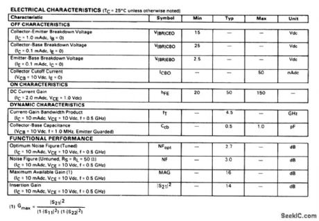
RF_bias_source
Published:2009/7/24 3:25:00 Author:Jessie


The BT500 shown in this circuit is designed for use in class-AB amplifiers to provide a thermally tracked bias source. The electrical characteristics are given in Fig. 2-44B. (View)
View full Circuit Diagram | Comments | Reading(654)
STEREO_MULTIPLEX_SUBCARRIER_GENERATOR
Published:2009/7/24 3:25:00 Author:Jessie

Double-sideband suppressed-carrier a-m subcarrier generator uses inverse feedback for low distortion. Double-modulcation system is used.-Modifying an F-M Transmitter for Compatible Stereo Multiplex, Electronics, 34:28, p 60-62. (View)
View full Circuit Diagram | Comments | Reading(889)
Liquid_flowmeter_thermally_based
Published:2009/7/24 3:25:00 Author:Jessie
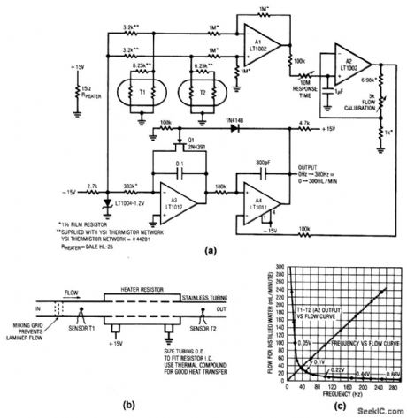
Fig. 14-3 This circuit shows a thermally based flowmeter, which features highly accurate rates as low as 1 mL/min and has a frequency output, which is a linear function of flow rate. This design measures the differential temperature between two sensors (Fig. 14-3B). Sensor T1, located before the heater resistor, assumes the fluid's temperature before the fluid is heated by the resistor. Sensor T2 picks up the temperature rise that is induced into the fluid by the resistor. The sensor difference signal appears at the Al output. A2 amplifies this difference with a time constant set by the response time adjustment. Figure 14-3C shows A2 output versus flow rate. The curves shown are for distilled water. To calibrate, set a flow rate of 10 mL/min and adjust the flow calibration trim for 10-Hz output. Linear Technology Linear Applications Handbook 1990 p AN5-6. (View)
View full Circuit Diagram | Comments | Reading(725)
CONSTANT_EXPOSURE_ENLARGER_TIMER_CIRCUIT
Published:2009/7/24 3:25:00 Author:Jessie

This circuit shows how to set up a NE555 timer to produce time steps proportional to f/stopsShown are values for switch-selected times of 2, 2. 8, 4 5. 6, etc, through 45 s for constant exposure with various enlarger lens settings. (View)
View full Circuit Diagram | Comments | Reading(688)
F_M_STEREO_DEMODULATOR
Published:2009/7/24 3:24:00 Author:Jessie
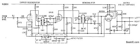
Signal from f-m discriminator is passed through 67-kc rejection fiber to control grid of 6AR8A as electronic switch, while high-amplitude 38-kc sine wave is applied to its deflection plates.One plate produces mainly left signed, and other produces mainly right signal. Cathode gives balanced L+R signal.-L. Solomon, Multiplex Adaptors for Compatible F-M Stereo Retention, Electronics, 34:33, p 45-.47. (View)
View full Circuit Diagram | Comments | Reading(724)
30_to_900_MHz_broadband_amplifier10_-V_supply
Published:2009/7/24 3:24:00 Author:Jessie

The electrical characteristics for the BFW92A shown in this circuit are given in Fig,2-43B. (View)
View full Circuit Diagram | Comments | Reading(772)
15_V_preset_output_controller
Published:2009/7/24 3:24:00 Author:Jessie

Figure 7-74 shows a MAX773 connected to provide 15-V output, with a 5-V input. This circuit is non-boot-strapped for minimum current consumption. See Fig. 7-68 for component suppliers. MAXIM NEW RELEASES DATA Book, 1995, P. 4-151. (View)
View full Circuit Diagram | Comments | Reading(634)
Nanopower_op_amp
Published:2009/7/24 3:21:00 Author:Jessie

The standby-power consumption, bandwidth, and slew rate (chapter 10) of this single-supply op amp are determined by the value of RSET, as shown in the table of Fig. 8-37B. Notice that the CA3440 is pin compatible with a 741, except that pins 1 and 5 (typically negative nulling pins) must be connected either directly to pin 4 or to a negative nulling pot. Also, pin 8, the ISET terminal, must be returned to either ground or -V via RSET. (View)
View full Circuit Diagram | Comments | Reading(598)
| Pages:1171/2234 At 2011611162116311641165116611671168116911701171117211731174117511761177117811791180Under 20 |
Circuit Categories
power supply circuit
Amplifier Circuit
Basic Circuit
LED and Light Circuit
Sensor Circuit
Signal Processing
Electrical Equipment Circuit
Control Circuit
Remote Control Circuit
A/D-D/A Converter Circuit
Audio Circuit
Measuring and Test Circuit
Communication Circuit
Computer-Related Circuit
555 Circuit
Automotive Circuit
Repairing Circuit