
Circuit Diagram
Index 1167
CONTRAST_METER
Published:2009/7/1 21:28:00 Author:May

Circuit Notes
One leg of the photocell (R1) is tied to the +15 volt supply and the other end is connected to ground through resistor R2, forming a voltage-divider network. The noninverting input of the 741 op amp, IC1, is tied to the junction formed by R1 and R2, while its inverting input is grounded through resistor R3. When switch S1is pressed, another divider network is formed, reducing the voltage applied to the inverting input of the op amp. When light hits the photocell its resistance begins to decrease causing a greater voltage drop across R2 and a higher voltage to be presented to the non-inverting input of IC1. This causes IC1 to output a voltage proportional to the two inputs. The circuit gives a meter reading that depends on the intensity of light hitting photocell R1; therefore, R1 should be mounted in a bottle cap so that the light must pass through a 3/16 inch hole. Potentiometer R5 is used to adjust the circuit for the negative you're working with. (View)
View full Circuit Diagram | Comments | Reading(681)
LOW_DISTORTION_LOW_LEVEL_AMPLITUDE_MODULATOR
Published:2009/7/1 21:27:00 Author:May
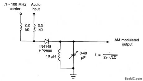
This simple diode modulator delivers excellent results when used for high percentage modulation at low signal levels. Constants are shown for a carrier frequency of about 10 MHz, but, with a suitable tank, the circuit will give good results at any frequency at which the diode approximates a good switch. To extend frequency above that for which the IN4148 is suited, a hot-carrier diode (HP2800, etc.) can be substituted. A shunt resistor across the tank circuit can be used to reduce the circuit Q so as to permit high percentage modulation without appreciable distortion. (View)
View full Circuit Diagram | Comments | Reading(3219)
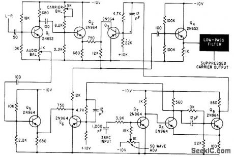
DOUBLE_SIDEBANDSUPPRESSED_CARRIER_RF_MODULATOR
Published:2009/7/1 21:26:00 Author:May

An RF input is applied to the primary of T1, which applies equal amplitude, opposite phase RF drive for output FETs Q1 and Q2. With no AF modulation at points A and B, the opposite phase RF signals cancel each other and no output appears at the 50 V output connector.When AF modulation is applied to points A and B, a modulated RF output is obtained. The dc stability and low frequency gain are improved by source resistors R18 and R19.A phase inverter consisting of a dual op amp (U1a and U1b) produces the out-of-phase, equal amplitude AF modulation signals. (View)
View full Circuit Diagram | Comments | Reading(695)
Portable_light_level_meter_with_five_decade_dynamic_range
Published:2009/7/24 3:02:00 Author:Jessie

This circuit operates from a single cell and is calibrated at midrange with appropriate illumination by adjusting R2 so that output equals the reference, and the meter is 'at center scale. In practical terms, adjust R6 and R2 so the output meter follows a standard light meter. Note that the log slope is not temperature compensated, so there might be error at the scale extremes. Also, silicon photodiodes (D1) are sensitive to near-infrared light, but ordinary film is not. So, an infrared-stop filter is recommended. A blue-enhanced photodiode for D1 or an appropriate correction filter will also produce excellent results. (View)
View full Circuit Diagram | Comments | Reading(602)
3_1_2_DIGIT_DVM(±2000_mV)COMMON_ANODE_DISPLAY
Published:2009/7/1 21:26:00 Author:May

View full Circuit Diagram | Comments | Reading(973)
0_to_500℃_furnace_exhaust_gas_temperature_monitor
Published:2009/7/24 3:14:00 Author:Jessie

Fig. 13-44 This circuit measures exhaust-gas temperature in a furnace. The 10-bit LTC1050 gives 0.5℃ resolution over a 0 to 500℃ range. The type-J thermocouple characteristic is linearized digitally inside the MCU. Linear interpolation between known temperature points spaced 30℃ apart introduces less than 0.1℃ error. The code for linearizing is available from Linear Technology. Linear Technology, Linear Applications Handbook 1990, p DN5-1. (View)
View full Circuit Diagram | Comments | Reading(558)
SUPPRESSED_CARRIER_SIGNAL_GENERATOR
Published:2009/7/24 3:14:00 Author:Jessie
Output of 38 kc, modulated by L-R signal, is obtained by bias-modulating symmetrical stable multivibrator. Carrier will remain suppressed 46 db below maximum signal level for days.-S. Feldman, Stereo F.M Multiplex Alignment Signal Generator, Electronics, 35:3, p 37-39. (View)
View full Circuit Diagram | Comments | Reading(985)
F_M_STEREO_MATRIXING
Published:2009/7/24 3:13:00 Author:Jessie
Matrixing is com pletely accomplished before detection. Can be substituted for 67-kc rejection filter of stereo demodulator. Also provides deemphasis.-L. Solomon, Multiplex Adaptors for Compatible F-M Stereo Reception, Electronics, 34:33, p 45-47. (View)
View full Circuit Diagram | Comments | Reading(781)
TWO_8_BIT_DACS_MAKE_A_12_BIT_DAC
Published:2009/7/1 21:25:00 Author:May

Two MC1408-8-bit D/A converters, A and B in the circuit diagram, are used. The four least significant bits of A are tied to zero. The four most significant bits of the 12-bit data are connected to the remaining four input pins. The eight least significant bits of the 12-bit data are connected to the eight input pins of B. The four most significant bits of the 12-bit data together have a weight of 16 relative to the remaining eight bits. Hence, the output from B is reduced by a factor of 16 and summed with the output from A using the summing op-amp configuration D. Voltage regulator chip, LM7236, is used to provide an accurate reference voltage, 2 V, for the MC1408. The full-scale voltage of the converter is 1/16 x 9.9609 + 1 x (9.375) or 9.9976 V. The step size of the converter is 2.4 mV. (View)
View full Circuit Diagram | Comments | Reading(2852)
3_1_2_DIGIT_TRUE_RMS_AC_VOLTMETER
Published:2009/7/1 21:24:00 Author:May

View full Circuit Diagram | Comments | Reading(2703)
ENLARGER_TIMER
Published:2009/7/1 21:24:00 Author:May


Circuit NotesThis precision, solid state, time delay circuit has delayed off and delayed on switch-ing functions that are interchangeably available by simply interchanging the relay contacts. (View)
View full Circuit Diagram | Comments | Reading(0)
DC_STATIC_SWITCHSCR_FIIP_FLOP
Published:2009/7/1 21:24:00 Author:May

This circuit is a static SCR switch for use in a dc circuit. When a low power signal is applied to the gate of SCR1, this SCR is triggered and voltage is applied to the load.The right hand plate of C charges positively with respect to the left hand plate through R1. When SCR2 is triggered on, capacitor C is connected across SCR1, so that this SCR is momentarily reverse biased between anode and cathode. This reverse voltage turns SCR1 off provided the gate signal is not applied simultaneously to both gates. The current through the load will decrease to zero in an exponential fashion as C becomes charged. (View)
View full Circuit Diagram | Comments | Reading(2193)
NOISE_IMMUNE_60_Hz_LINE_SYNC
Published:2009/7/1 21:23:00 Author:May

View full Circuit Diagram | Comments | Reading(492)
POWER_ON_RESET
Published:2009/7/1 21:22:00 Author:May

A reset pulse is often required at power-on in a digital system. This type of reset pulse is ideally provided by this circuit. Because of the high input imp-edance of the Schmitt trigger, long reset pulse times may be achieved without the excess dissipation that results when both output devices are on simultaneously, as in an ordinary gate device (B). (View)
View full Circuit Diagram | Comments | Reading(4029)
Linearized_platinum_RTD_thermometer_single_supply
Published:2009/7/24 3:13:00 Author:Jessie

Fig. 13-43 In this circuit, an LM392 comparator/op amp (A1 and C1) is used to provide both gain and linearization for a platinum RTD in a single-supply thermometer, which measures from 0 to 500℃ with ±1℃ accuracy. To calibrate, substitute a precision resistance box for the sensor, adjust 0℃ for 0.10-V output (with the box set to 1000 ohms). Next, set the box to 2846Ω (500℃) and adjust the 1-kΩ gain trim for an output of 2.6 V. Repeat the adjustments until both zero and full-scale are fixed. National Semiconductor Linear Applications Handbook 1991 p 838. (View)
View full Circuit Diagram | Comments | Reading(783)
SHIFT_REGISTER
Published:2009/7/1 21:21:00 Author:May

The shift pulse amplitude is less than 15 volts. If a stage is off, the shift pulse will no, be coupled to the next stage. If it is on, the diode will conduct triggering the next stage. Just prior to the shift pulse the anode supply is interrupted to turn off all stages.The stored capacitor charge determines which stages will be retriggered. (View)
View full Circuit Diagram | Comments | Reading(2121)
12_V_preset_output_high_efficiency_controller_boot_strapped
Published:2009/7/24 3:12:00 Author:Jessie

Figure 7-69 shows a MAX771 connected to provide 12-V output at 0.5 A, with a 5-V input.See Fig.7-68 for component suppliers. MAXIM NEW RELEASES DATA Book 1995, P.4-150. (View)
View full Circuit Diagram | Comments | Reading(603)
Single_cell_noninverting_20_dB_amplifier
Published:2009/7/24 3:12:00 Author:Jessie

This circuit is identical to that of Fig. 8-33, except that the output is noninverting. (View)
View full Circuit Diagram | Comments | Reading(601)
ALARM_FOR_SPECTRUM_ANALYZER
Published:2009/7/1 21:21:00 Author:May

Circuit drives audible alarm when frequency of interest appears in spectrum range. Display cursor can be preset to initiate narrow search band in which fx is expected to appear. 100-μs pulse representing cursor position in display sweep triggers mono IC1 so its output becomes window whose time-out is equivalent to band in which fx is center. Comparator A1 supplies high output when fx appears. Simultaneous arrival of this signal and timer window at gate A sets output of left flip-flop high. At end of window period, right flip-flop also goes high and initiates alarm via Q1. Loss of fX stops alarm.-R. L. Messick, Alarm Simplifies Spectrum-Analyzer Measurements, EDN Magazine, JuneS, 1978, p 152. (View)
View full Circuit Diagram | Comments | Reading(695)
STEREO_MULTIPLEX_F_M_SIGNAL_GENERATOR
Published:2009/7/24 3:12:00 Author:Jessie
Used for testing and aligning multiplex receivers and adapters. Switches permit generating L+R or L-R separately with or without preemphasis and inserting or re moving SCA 67-kc signal.-S. Feldman, Stereo F-M Multiplex Alignment Signal Generator, Electronics, 35:3, p 37-39. (View)
View full Circuit Diagram | Comments | Reading(3057)
| Pages:1167/2234 At 2011611162116311641165116611671168116911701171117211731174117511761177117811791180Under 20 |
Circuit Categories
power supply circuit
Amplifier Circuit
Basic Circuit
LED and Light Circuit
Sensor Circuit
Signal Processing
Electrical Equipment Circuit
Control Circuit
Remote Control Circuit
A/D-D/A Converter Circuit
Audio Circuit
Measuring and Test Circuit
Communication Circuit
Computer-Related Circuit
555 Circuit
Automotive Circuit
Repairing Circuit