
Circuit Diagram
Index 1174
PULSE_WIDTH_DETECTOR
Published:2009/7/1 19:52:00 Author:May

Connections as shown for 555 timer give output only if trigger pulse width is greater than time constant (t2 = 1.1RtCt) of mono MVBR circuit. Q1 is normally off. Pin 2 of 555 is then high. At start of trigger pulse, output at point C is low. Positive trigger drives Q1 on for time determined by R1C1, feeding negative-going pulse to trigger pin 2. Timer then acts as normal mono, driving Q2 on for time t2. If input pulse is still high at end of t2, it appears at output D since Q2 is now off. Output pulse width is thus equal to input trigger width less 1.1RtCt. For greater accuracy, insert delay between point A and R4 equal to inherent propagation delay of timer.-S. Sarpangal, Build a Pulse-Width Detector with a 555 Timer, EDN Magazine, Oct. 5, 1977, p 93 and 96. (View)
View full Circuit Diagram | Comments | Reading(0)
Humidity_to_frequency_converter
Published:2009/7/24 3:30:00 Author:Jessie
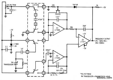
Fig. 14-6 This circuit converts the output of a relative-humidity (RH) transducer into a calibrated frequency output, using an LTC1043 switched-capacitor IC. To calibrate, place the transducer in a 5% RH environment, and adjust the 5% RH trim for 50-Hz output. Next, place the transducer in a 90% RH environment, and adjust the 90% RH trim for a 900-Hz output. Repeat this procedure unti1 both points are fixed. Relative humidity accuracy will be 2% over the 5%-90% RH range. If RH standards are not available, the circuit can be approximately calibrated with fixed capacitors in place of the transducer. Ideal values are 5% RH=379.3 pF and 90% = 523.8 pF. Note that these values assume an ideal sensor. An actual device can depart from the values by as much as 10%. Linear Technology Linea Applications Handbook 1990 p AN7-11. (View)
View full Circuit Diagram | Comments | Reading(636)
Basic_meter_amplifier
Published:2009/7/24 3:30:00 Author:Jessie

This circuit operates from two D cells, and provides a current range as low as 100 nA full-scale. With RS set at 10 MΩ, the total current drain is 0.6 μA for a total power-supply drain of 1.8 μW. Input bias current is about 600 pA. When operated with two No. 950 D cells (Eveready), quiescent power drain is so low that no on/off switch is needed (typically, batteries last for a minimum of one year).Meter deflection is set by the value of Rf, where output voltage VO, equals If/Rf. A practical value for full-scale meter deflection is 300 mV. (View)
View full Circuit Diagram | Comments | Reading(697)
Linearized_methane_transducer_signal_conditioner
Published:2009/7/24 3:28:00 Author:Jessie
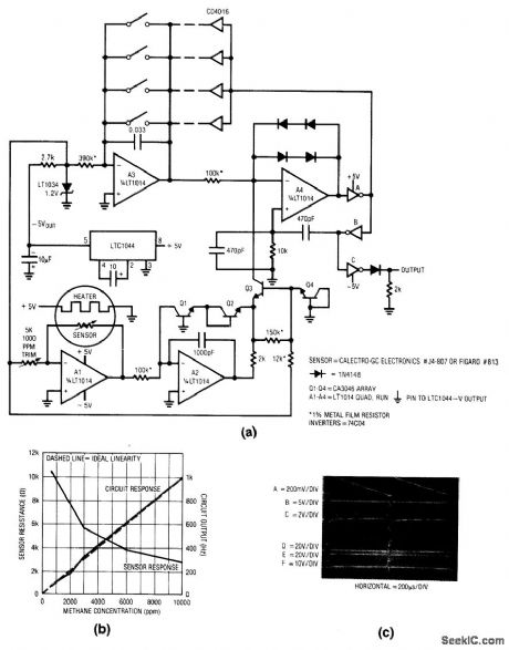
Fig. 14-5 The frequency output of this circuit is directly proportional to the methane concentration detected by the transducer. Figure 14-5B shows the transducer versus circuit response. To calibrate, place the transducer (sensor) in a 1000-pprn methane environment, and adjust the 1000-ppm trim for a 100-Hz output. Accuracy from 500 to 10,000 ppm is limited by the sensor 10% specification. Linear Technology, Linear Applications Handbook 1990. p AN11-3. (View)
View full Circuit Diagram | Comments | Reading(605)
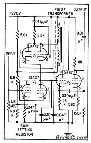
135_VDC_SUPPLY
Published:2009/7/24 3:28:00 Author:Jessie

This supply can be used for vacuum-tube experiments. It uses a 120:120 Vac isolation trans-former to isolate the ac line from the dc output. T1 can be 30- to 100-mA capacity and C1 is a 40-μF 250-V electrolytic. (View)
View full Circuit Diagram | Comments | Reading(753)
500_nW_x_10_amplifier
Published:2009/7/24 3:28:00 Author:Jessie

This circuit has a quiescent power dissipation of 470 nW, with a slew rate of 1 V/ms for a 0.05-μA set current. The 3-dB down (gain of -7.07) frequency for the circuit is about 300 Hz. Peak-to-peak output swing into a 100-kΩ load is 0.7 V or ±0.35 V peak. An increase in supply voltage to ±1.35 V (such as two mercury cells) increases the output swing by ±0.35 V to 1.4 V peak-to-peak. This increases the power dissipation to about 1 μW per cell, a power drain of 15 μW or less will not affect the shelf life of a mercury cell. (View)
View full Circuit Diagram | Comments | Reading(752)
RE_bias_source_SOE_style_tpacknge
Published:2009/7/24 3:28:00 Author:Jessie


The BT500F shown in this circuit is designed for use in class-AB amplifiers to provide a thermally tracked bias source. The electrical characteristics are given in Fig. 2-45B. (View)
View full Circuit Diagram | Comments | Reading(627)
16_V_preset_output_controller
Published:2009/7/24 3:27:00 Author:Jessie

Figure 7-75 shows a MAX773 connected to provide 16-V output, with a 5-V input. This circuit is boot-strapped for operation with inputs less than 5 V. See Fig. 7-68 for component suppliers. MAXIM NEW RELEASES DATA Book, 1995, P. 4-15t. (View)
View full Circuit Diagram | Comments | Reading(598)
Thermal_anemometerair_flowmeter
Published:2009/7/24 3:27:00 Author:Jessie

Fig. 14-4 This circuit provides a voltage output that corresponds to airflow. The circuit operates by measuring the energy required to maintain a heated resistance wire at constant temperature. The sensor is a type 328 lamp with the glass envelope removed. The lamp is placed in a bridge monitored by A1. The A1 output is amplified by Q1 and fed back to the bridge. When power is applied, the lamp is at low resistance and the Q1 emitter tries to go full-on. As current flows through the lamp, the filament temperature rises quickly, which increases filament resistance. This increases the A1 negative input. A1 acts to balance the bridge by applying more current through Q1. Thus, the voltage at the Q1 emitter is predictably related to airflow past the lamp. The remaining circuits square and amplify the Q1 emitter voltage to give a linear, calibrated output versus airflow rate, To calibrate, place the lamp in the air flow so that the filament is at a 90° angle to the flow. Next, either shut off the air flow or shield the lamp from the flow, and adjust the zero flow for a circuit output of 0 V. Then, expose the lamp to air flow of 1000 ft/min and adjust the full-scale flow for 10-V output. Repeat these adjustments until both points are fixed. With this calibration, the air flowmeter is accurate within 3% over the entire 0- to 1000-ft/min range. Linear Technology Linear Applications Handbook, 1990, p. AN5-7.
(View)
View full Circuit Diagram | Comments | Reading(2757)
PIN_DIODE_PROVIDES_120_DB_ACC_RANGE
Published:2009/7/24 3:26:00 Author:Jessie
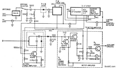
Dynamic signal range exceeds 120 db in fully transistorized Fisher TFM-1000 stereo set. Will receive signals as low as 1.5 microvolts without distortion, yet 0.5-V signals can be handled without overload or spurious response. Solid-state pin diode servos as gain-controlled attenuator. Separate 10.7-Mc tuned amplifier delivers agc voltage that, along with d-c amplifier, controls pin diode. Action of tuned amplifier is delayed until antenna signal is 1 mV.-F. L. Mergner, P-i-n Diode und FET's Improve F-M Reception, Electronics, 39:17, p 114-118. (View)
View full Circuit Diagram | Comments | Reading(846)
Three_terminal_regulation_with_remote_sensing
Published:2009/7/24 4:51:00 Author:Jessie

This circuit allows the regulator to remotely sense the feedback voltage and eliminate the effects of voltage drop in the supply lines. This is useful where high currents must be transmitted over relatively long supply lines or PC rails. A1 senses the voltage at the point of load. The A1 output, summed with the regulator output, modifies the adjustment pin voltage to compensate for the voltage lost across RDROP. The feedback divider is returned through a separate lead from the load. (View)
View full Circuit Diagram | Comments | Reading(793)
EIGHI_TRANSISTOR_MVBR
Published:2009/7/24 4:51:00 Author:Jessie
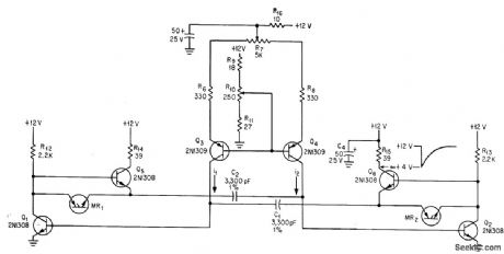
Emitter-followers Q5 and Q6 increase gain by providing low. impedance path for recharging timing capacitors. R7 controls mark/space ratio and R10 controls frequency.-C. J. Dakin, Novel Multivibrators Test Tape Transports, Electronics, 37:7, p 40-43. (View)
View full Circuit Diagram | Comments | Reading(785)
BiMOS_LED_bar_graph_driver
Published:2009/7/24 4:50:00 Author:Jessie

Fig. 15-31 In this circuit, the LED for a particular comparator is turned on when the input voltage reaches the voltage on the resistor-driver reference.Because of the MOSFET input(and bipolar output)this circuit is ideal where input-signal loading is critical-even though many comparator inputs are driven In parallel.Figures 15-30B and 15-30C show the pin connections and electrical characteristics, respectively. Harris Semiconductor Linear&Telecom IC. 1991, p. 4-23. (View)
View full Circuit Diagram | Comments | Reading(887)
25_75_KC_FREQUENCY_MODULATOR
Published:2009/7/24 4:50:00 Author:Jessie
Frequency changes are linear within 1% with changes in input voltage. Circuit can easily be modified for other frequency ranges. Designed for use with magnetic tape recorders. Cf is primary frequency-determining element.-P. S. Bengston, Frequency Modulator Covers 25.75 Kc, Electronics, 31:31, p 100-106. (View)
View full Circuit Diagram | Comments | Reading(813)
BiMOS_window_comparator
Published:2009/7/24 4:50:00 Author:Jessie


Fig. 15-30 In this circuit, the LED is turned on whenever the input signal is above the lower limit (VL) but below the upper limit (VU), as determined by the R1/R2/R3 divider. Figures 15-30B and 15-30C show the pin connections and electrical characteristics, respectively. Harris Semiconductor Linear & Telecom ICs, 1991 p 4-15, 4 18 4-22. (View)
View full Circuit Diagram | Comments | Reading(586)
MAG_TAPE_PRINT_THROUGH_SUPPRESSOR
Published:2009/7/24 4:50:00 Author:Jessie
Echoes occurring before and after true signal in recorded magnetic tape stored for some lime, called print-through, and noticeable chiefly during soft musical passages and during recorded speech or singing, are sup pressed by biased. diode type of quieting are that silences audio channel whenever signal drops to 40 db below peak. Each diode is back-biased 0.1 V. If program peaks are 10 V, diodes become nonconducting for all signals more than 40 db below this peak. To prevent loss of desired signal near the zero axis, signals above the threshold are amplified, recti0ed, filtered, and used in time-constant circuit to keep diodes conducting throughout each spoken word.-D. Cronin, Squelch Circuit Mutes Magnetic Tape Echoes, Electronics, 31:19, p 66-67. (View)
View full Circuit Diagram | Comments | Reading(828)
RECORDING_AMPIJFIER
Published:2009/7/24 4:49:00 Author:Jessie
Has sufficient input impedance for medium-high-impedance magnetic microphone. Includes equalization to produce flat response with Nortronics low-impedance recording head when playback preamp is adjusted for NAB equalization at tape speed of 7.5 inches per second.- Transistor Manual, Seventh Edition, General Electric Co., 1964, p 272. (View)
View full Circuit Diagram | Comments | Reading(1860)
Zero_crossing_detector_single_supply
Published:2009/7/24 4:48:00 Author:Jessie

Fig. 15-29 This circuit is similar to that of Figs. 15-2, 15-7, 15-9, 15-15, and 15-17, but it uses only one section of an LP165/365 and it requires a single supply. Figures 15-24B and 15-24C show the pin connections and electrical characteristics, respectively. Raytheon Linear Integrated Circuits, 1989, p. 5-40. (View)
View full Circuit Diagram | Comments | Reading(887)
BATTERY_OPERATED_DICTATING_MACHINE
Published:2009/7/24 4:47:00 Author:Jessie
Amplifier voltage is regulated by Q5 and zener diode. Q6 functions as on-off switch controlled either by microphone switch or by metallic coating at both ends of two-track tape.-L. Hannemann, Pocket-size Dictating Machine, Electronics, 33:44, p 73. (View)
View full Circuit Diagram | Comments | Reading(758)
Increasing_three_terminal_regulator_stability
Published:2009/7/24 4:47:00 Author:Jessie

This circuit shows a way to increase the stability of regulator output over time and temperature. The circuit is particularly useful in powering strain-gauge transducers (chapter 14). The output voltage is divided down and compared to the 2.5-V reference by A1, which, in turn, forces the adjustment pin to whatever voltage is required to maintain the 10-V output. (View)
View full Circuit Diagram | Comments | Reading(712)
| Pages:1174/2234 At 2011611162116311641165116611671168116911701171117211731174117511761177117811791180Under 20 |
Circuit Categories
power supply circuit
Amplifier Circuit
Basic Circuit
LED and Light Circuit
Sensor Circuit
Signal Processing
Electrical Equipment Circuit
Control Circuit
Remote Control Circuit
A/D-D/A Converter Circuit
Audio Circuit
Measuring and Test Circuit
Communication Circuit
Computer-Related Circuit
555 Circuit
Automotive Circuit
Repairing Circuit