
Circuit Diagram
Index 1166
PIANO_TONE_GENERATOR
Published:2009/7/1 21:41:00 Author:May
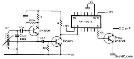
RF oscillator combined with General Instrument AY-1-0212 IC mastertonegenerator replaces 12 conventional RC oscillators otherwise required in electronic piano. Frequencies generated are within 0.1% of equal-temperament scale, so piano will work well without being tuned. Three-part article gives all circuits and construction details for simple portable touch-sensitive electronic piano.-G, Cowie, Electronic Piano Design, Wireless World, Part 3, May 1974, p 143-145. (View)
View full Circuit Diagram | Comments | Reading(1918)
MULTIPLEXING_LED_DRIVERS
Published:2009/7/1 21:41:00 Author:May

Duty cycle of each display digit can be varied from 10% (full on with strobing) to less than 1% (almost off).Circuit uses 7490 and 7442 as 1-of-10 multiplex driver to strobe cathodes of display digits through Q1, Q3, etc and tum on required 7400 multiplex gate through Q2, Q4, etc. Outputs of7447 are polarity-inverted by QA, QB, etc, which can be Sylvania ECG 159 rated at 200 mA. Q1,Q3, etc can be EGG 123 or HEP S0002, while Q2, Q4, etc can be any silicon PNP transistor.-B.Hart, Cument-Saver Counter Display, 73 Magazine, June 1977, p 174-176. (View)
View full Circuit Diagram | Comments | Reading(2215)
SPEED_ALARM
Published:2009/7/1 21:39:00 Author:May

Frequency detector using two IC timers provides alarm output when input frequency is greater than reference frequency, corresponding to overspeed. Calibrated mono MVBR A1 produces fixed-width positive pulse across R2, with average voltage of pulse varying linearly with input pulse train frequency. ComparatorA2 changes states when integrated output of R3-C1 on pin 5 goes above or below 2-V voltage threshold of A2. With values shown, desired frequency is 1 kHz and circuR detects frequency variation of less than 1%. If low-frequency alarm is desired, connect logic input pin 2 of A2 to reference voltage (pin 4) instead of to ground.-W. G. Jung, IC Timer Cookbook, Howard W. Sams, Indianapolis, IN, 1977, p 228-230. (View)
View full Circuit Diagram | Comments | Reading(0)
SINGLE_STEPS_AT_100_KC
Published:2009/7/24 3:05:00 Author:Jessie
Tunnel-diode step generator provides single 400-my steps that are fast and free from overshoot, for testing wideband systems. Flat top of step, used for tests, is 2 microsec long. Step can be triggered with 0.5-V signal at repetition rates to 100 kc, or can free-run at about 100 kc.-R.Carlson, Tunnel-Diode Fast-Stop Generator Produces Positive or Negative Steps, Electronics, 34:30, p 48-49. (View)
View full Circuit Diagram | Comments | Reading(506)
SOUND_TRIGGER_FOR_FLASH_UNIT
Published:2009/7/1 21:38:00 Author:May

Circuit NotesThe circuit is based on operational amplifier IC1 used in the noninverting amplifier mode. R1 and 2 set the gain at about 500. RV1 (sensitivity) biases the noninverting input to the negative supply. Q1 provides the relatively high trigger current required by the triac. When a signal is received by the microphone, the signals are amplified (by IC1).The triac is triggered and a low resistance appears across its A1 and A2 terminals which are connected via the flashlead to the strobe. The circuit operates almost instantly, giving very little delay between the commencement of the sound and the flashgun being triggered. (View)
View full Circuit Diagram | Comments | Reading(919)
PWM_BRIGHTNESS_CONTROL
Published:2009/7/1 21:37:00 Author:May

Single TTL IC combines functions of oscillator and modulator to provide intensity control of solid-state display by pulse-width modulation. Fan-out of 10 is available from Q output, suitable for displays such as Hewlett-Packard 7300 series, and smaller fan-out is available from other Q terminal.-C. Bartram, P.W.M. Oscillator to Vary Display-Intensity, Wireless World, March 1976, p 89. (View)
View full Circuit Diagram | Comments | Reading(1239)
RANDOM_MUSIC
Published:2009/7/1 21:37:00 Author:May

Uses Johnson counter as special shift register producing almost random bit patterns of 18 to 3255 12-bit words under control of clock operating in range of about 1-10 Hz. Oscillator (upper right) uses NE555 as voltage-controlled square-wave generator playing one of eight musical notes (C. D. E. F. G. A. B. or C), depending on state of seven noteselector lines coming from selector switches. Oscillator is divided down in frequency by three-stage ripple counter to provide four octaves of range. R1 -R8 serve fortuning each note to pitch. Outputs 8F and 2F are paired to drive left input of stereo amplifier, while outputs 16F and 4F are similarly paired for right channel. Article covers construction, tune-up, and creation of pleasing musicalsequences.-D. A. WalIace. The Sound of Random Numbers. 73 Mag-azine. Feb. 1976, p 60-64. (View)
View full Circuit Diagram | Comments | Reading(825)
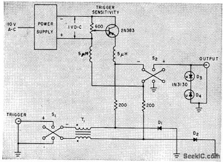
SIMPLE_SYNCHRONIZED_SLAVE_PHOTO_FLASH
Published:2009/7/24 3:04:00 Author:Jessie

A light-activated silicon-controlled rectifier (Q1) is triggered by a flash of light from the master flash unit. (View)
View full Circuit Diagram | Comments | Reading(659)
ELECTRONIC_FLASH_TRIGGER
Published:2009/7/1 21:35:00 Author:May

Circuit NotesA negative pulse at the input is fed via capacitor C1 to the input pin (2) of the IC.Pin 2 is held slightly above its triggering voltage of 1/3 Vcc, by the voltage divider comprising R1, R2 and RV1. The negative pulse triggers the IC and the output (pin 3) goes high for a time period controlled by RV2, R3 and C2. When the output goes low again at the end of the time interval, capacitor C3 charges through the gate cathode circuit of the SCR switching it on and firing the flash. Capacitor C1 isolates the input from the voltage divider so that the unit isn't sensitive to the dc level at the input. RV1 acts as a sensitivity control by allowing the voltage to be adjusted to a suitable level so that the input signal will trigger the IC. Resistor R4 limits the discharge current from C2 at the end of the timing cycle protecting the IC. The LED and its protective resistor R5 act as an indicator to show that the unit has triggered, simplifying the setting up process and minimizing the number of times the strobe has to be fired. This means that the strobe needn't be fired until a photo is to be taken. (View)
View full Circuit Diagram | Comments | Reading(725)
TTL_OSCILLATOR_INTERFACES_DATA_FOR_DISPLAY_BY_A_TELEVISION_SET
Published:2009/7/1 21:32:00 Author:May

Three gates of a 74LS04 form the oscillator circuit. Capacitor C1 allows fine-frequency adjustment to a specific television channel and helps stabilize the circuit. Potentiometer R1 acts as the mixing input and provides adjustment of the contrast ratio for the best viewing. A fourth gate buffers and helps stabilize the oscillator. (View)
View full Circuit Diagram | Comments | Reading(587)
Single_cell_electronic_thermometer
Published:2009/7/24 3:04:00 Author:Jessie

This circuit is useful in the range from -55°C to 150°C. Sensor S1 develops a current that is proportional to absolute temperature so that the readout could be in °F, rather than in °C, by trimming R2 and R3. With the values shown, readout is from 0° to 100°C. Refer to chapter 13 for information on temperature scales and absolute temperature. (View)
View full Circuit Diagram | Comments | Reading(615)
VIDEO_MODULATOR
Published:2009/7/1 21:32:00 Author:May

This circuit permits direct connection of composite video signals from video games and microcomputers to the antenna terminals of TV sets. The output signal level is controlled by the modulation input. (View)
View full Circuit Diagram | Comments | Reading(1)
150_MHz_100_W_amplifier_28_V_supply
Published:2009/7/24 3:03:00 Author:Jessie
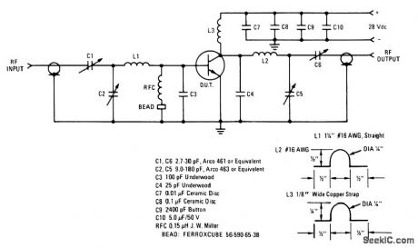
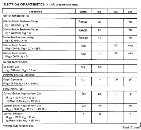
The electrical characteristics for the 2N6166 shown in this circuit are givenin Fig. 2-38B. (View)
View full Circuit Diagram | Comments | Reading(907)
SEGMENTED_SWEEP_DISPLAY
Published:2009/7/24 3:03:00 Author:Jessie

Staircase voltage builds up across C2 when pulses from Q2 turn Q3 on momentarily. R3 controls voltage amplitude of each step. R1 controls rate of free-running oscillator tube.-J. E.Russell, Ten Signals at a Glance, Electronics, 37:19, p 54-57. (View)
View full Circuit Diagram | Comments | Reading(824)
Proportional_temperature_controller_1
Published:2009/7/24 3:03:00 Author:Jessie

Fig. 13-37 This circuit provides proportional temperature control with optical isolation and synchronized zero crossing. Proportional control is provided by an LM122 timer, although the timing function is not used. Instead, the trigger terminal is held high and the LM122 is used as a high-gain comparator with a built-in reference. R2 sets the temperature to be controlled by R1. R5 and R7 set the width of proportioning band and can be scaled as necessary to alter the band width (larger resistors made the band narrower). The values shown give about a 1℃ band. R4 and C1 set the proportioning frequency, which is about 1 Hz with the values shown. R12, R13, and D2 produce the synchronized zero-crossing feature by preventing Q1 from turning off after the voltage across Q2 has climbed above 2.5 V. Any unregulated supply between 6 and 15 V is satisfactory. National Semiconductor Linear Applications Handbook 1991 p 337. (View)
View full Circuit Diagram | Comments | Reading(1441)
DARKROOM_EXPOSURE_TIMER
Published:2009/7/24 3:02:00 Author:Jessie


In this circuit, op-amp IC1b and timer IC2 form a voltage-controlled oscillator circuit with its frequency varied by the dual-ganged potentiometer (VR1). Resistor R3 effectively swamps any variations in VR1 value, preventing them from altering the lowest control voltage, as set by R4 and R5. The values of these resistors are chosen to give a ratio between the highest and lowest volt-ages of 32.5:1, which sets the timing range from 0.4 to 13 minutes, ensuring cover of the intended range of 0.5 to 12 minutes. Opamp IC1b is used as a comparator. Capacitor C1 charges in exponential fashion from VR2 and R6 until the voltage across it reaches the selected control voltage from VR1b. When it does so, the output of IC1b goes low, triggering timer IC2, which then delivers a 2.5-ms pulse from output pin 3. This is used to discharge C1 via transistor TR1. VR2 provides the overall trimming adjustment for calibration. From IC2, the output pulses are applied through resistor R10 to the CLOCK input of binary counter IC3. This counts the pulses until the selected output goes high, blocking the CLOCK signal via diode D1. Pin 15 of IC3 is the 11th counter output, so 1024 clock pulses are counted. The final output of the circuit is controlled by quad NOR gate IC4. When the cir-cult is first energized, a positive pulse from C5 via D2 to IC4a pin 1 causes IC4a output pin 3 to go low and IC4b output pin 4 to go high, the OFF state. The high output of IC4b pin 4 charges C4 through R13. When START switch S1 is pressed, output pin 3 goes high, the ON state. At the same time, the pulse resets counter IC3 via its input, pin 11. Capacitor C4 will not be recharged until the output re-turns to the OFF state, ensuring that if switch S1 is held down or accidentally pressed again before timing is complete, the output time will not be affected. Timing ceases when the link-selected output of IC3 goes high and resets IC4a through R14. (View)
View full Circuit Diagram | Comments | Reading(710)
12_BIT_DAC_WITH_VARIABLE_STEP_SIZE
Published:2009/7/1 21:31:00 Author:May

The step size of the converter is variable by selection of the high order data bits.The first DAC, A, has a stable reference current supplied via the 10.24 V reference IC and R1. R2 provides bias cancellation. As shown, only the first 4 MSB inputs are used, giving a step size of225/256 x 2.048/16 = 0.127 mA. This current supplies the reference for DAC B whose step size is then 0.1275/256 = 0.498 μA. Complementary voltage outputs are available for unipolar output and using R3 = R4 = 10 K, Vout is ±10.2 V pproximately, with a step size (1 LSB) of approximately 5 mV. If desired an op amp can be added to the output to provide a low impedance output with bipolar output symmetrical about ground, if R5 = R6 within 0.05%. Note that offset null is required, and all resistors except R2 and R3 should be 1% high stability types.By using lower order address lines than illustrated for DAC A, a smaller step size (and therefore full-scale output) can be obtained. Unused high order bits can be manipulated high or low to change the relative position of the full-scale output. (View)
View full Circuit Diagram | Comments | Reading(932)
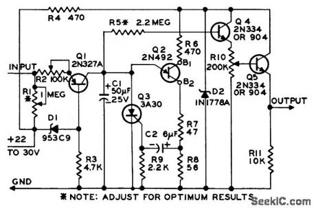
PlANO_MUSIC_FROM_ORGAN
Published:2009/7/1 21:29:00 Author:May


Simple add-on circuit for electronic organ attenuates output of oscillator exponentially to zero in manner suitable for mimicking waveform of piano. Circuit is self-triggering, so exponential decay starts only when output of multivibrator is applied; this eliminates need for extra contacts on key-board. With no input, Tr1 is on and point A is at supply voltage. Input signal turns Tr1 off, discharging C3 through R3 and R5. Voltage across C3 controls gate of FET, with R5 being adjusted so FET just switehes off when C3 is fully discharged. Tr1 then conducts and C3 charges rapidly, to permitfast piano playing.-C. J. Outlaw, Electronic Organ to Piano, Wireless World, Feb.1975, p 94. (View)
View full Circuit Diagram | Comments | Reading(933)
VIDEO_MODULATOR_CIRCUIT
Published:2009/7/1 21:28:00 Author:May

These are modulator circuits for modulation of video signals on a VHF/UHF carrier.The circuits require a 5V power supply and few external components for the negative modulation mode. For positive modulation an external clamp circuit is required. The circuits can be used as general-purpose modulators without additional external components. The IC is TDA6800. (View)
View full Circuit Diagram | Comments | Reading(710)
LOW_FREQUENCY_STAIRSTEP
Published:2009/7/24 3:02:00 Author:Jessie
Accepts pulse input, either random or evenly spaced, and produces output ofter fixed number of inputs. Useful in measuring and recording low. frequency data. Pulse widths may be 1 millisec to several hundred millisec. Output may have anywhere from 2 to 1,000 steps.By making R1 smaller and eliminating R2, output becomes sawtooth with 1% linearity, variable from 10 millisec to 15 minutes depending on values of C1 and R1.-Low.Frequency Stairstep Generator and Timing Circuit, Electronic Circuit Design Handbook, Mactier Pub. Corp., N.Y., 1965, p 144. (View)
View full Circuit Diagram | Comments | Reading(579)
| Pages:1166/2234 At 2011611162116311641165116611671168116911701171117211731174117511761177117811791180Under 20 |
Circuit Categories
power supply circuit
Amplifier Circuit
Basic Circuit
LED and Light Circuit
Sensor Circuit
Signal Processing
Electrical Equipment Circuit
Control Circuit
Remote Control Circuit
A/D-D/A Converter Circuit
Audio Circuit
Measuring and Test Circuit
Communication Circuit
Computer-Related Circuit
555 Circuit
Automotive Circuit
Repairing Circuit