
Circuit Diagram
Index 1178
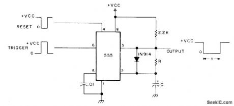
INVERTED_MONO
Published:2009/7/1 20:03:00 Author:May
Connection shown for 555 timer accepts positive trigger pulses and delivers negative output pulses. Duty cycies above 99% are possible without jitter. Heavy loads can be driven from pin 7 without loss of accuracy, but excessive loading of pin 3 can affect timing accuracy. Width of output pulse is 1 ms for values of R1 and C1 shown. Trigger must be held, below two-thirds of supply voltage for standby I and raised above two-thirds of supply momentarily (not longer than pulse width) for triggering.-W. G. Jung, IC Timer Cookbook, Howard W. Sams, Indianapolis, IN, 1977, p 89. (View)
View full Circuit Diagram | Comments | Reading(681)
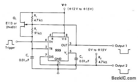
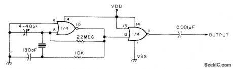
VARIABLE_DUTY_CYCLE
Published:2009/7/1 20:02:00 Author:May

First section of Exar XR-2556 dual timer operates as astable MVBR whose frequency is equal to 1.44/(RA + 2RB)C1, with output used to trigger timer 2 connected in monostable mode. Time delay T2 of timer 2 is made less than period of timer 1 waveform, so both timers have same frequency. Duty cycle is determined by timing cycle of timer 2, adjustable from 1% to 99% with R2. Supply voltage is 4.5-16 V.- Timer Data Book, Exar Integrated Systems, Sunnyvale, CA, 1978, p 23-30. (View)
View full Circuit Diagram | Comments | Reading(1594)
GATE_DIPPER__1
Published:2009/7/1 20:01:00 Author:May

Solid.state-version of vacuumtube grid-dip meter gives dip from 50 to about 20 pA on most bands in range of 1.8 to 150 MHz when dipper is held 1 inch away from resonant circuit under test. Uses Siliconix 2N5398 UHF JFET, but MPFl07 (2N5486) can also be used.Coil tap position is more critical at higher frequencies; adjust tap for most pronounced dip.Article gives coil data for five frequency ranges.-C. G. Miller, Gate-Dip Meter, Ham Radio, June 1977, p 42-43. (View)
View full Circuit Diagram | Comments | Reading(3217)
PROGRAMMABLE_ASTABLE
Published:2009/7/1 20:00:00 Author:May
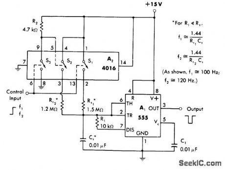
4016 CMOS analog switch selects 1.5-megohm timing resistor Rt1 when control input line is high, to give negative-going 100-Hz output pulses. When input is low, CMOS switch S2 is on, selecting 1.2-meg-ohm timing resistor Rt2 to give 120-Hz output.-W. G. Jung, IC Timer Cookbook, Howard W. Sams, Indianapolis, IN, 977, p 136-137. (View)
View full Circuit Diagram | Comments | Reading(1149)
1_Hz_TO_1_MHz
Published:2009/7/1 19:59:00 Author:May

Opamp-based astable MVSR generates square waves over extremely wide range, with suitable changes in circuit values. RCA 3130 opamp has CMOS output stage for driving either 5-V TTL or 10-15 V CMOS logic stages directly. Values are for 100 Hz. R1 and C1 can be readily scaled for different ranges. To control symmetry, replace Rt with two resistors in series with reverse-connected diodes as at lower right.-W. Jung, An IC Op Amp Update, Ham Radio, March 1978, p 62-69. (View)
View full Circuit Diagram | Comments | Reading(2071)
LOW_POWER_MONO
Published:2009/7/1 19:58:00 Author:May
555 timer provides low-drain monostable operation suitable for inter-facing with CMOS 4011B NAND gates. Standby drain is less than 50μA. When mono is on, cur-rent drawn is 4.5 mA for pulse duration of T = 1.1RC.- Signetics Analog Data Manual, Signetics, Sunnyvale, CA, 1977, p 733. (View)
View full Circuit Diagram | Comments | Reading(777)
555_ASTABLE
Published:2009/7/1 19:57:00 Author:May
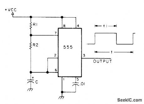
Produces repetitive rectangular output at frequency equal to 1.443/(R1 + 2R2)C hertz. Duty cycle is determined by values of R1 and R2; R2 must be much larger than R1 to obtain nearly a 50% duty cycle. Normal range for duty cycle is S1 to 99%. VCC is 4.5-16 V at 3-10 mA.-H. M. Berlin, IC Timer Review, 73 Magazine, Jan. 1978, p 40-45. (View)
View full Circuit Diagram | Comments | Reading(2465)
ASTABLE_OSCILLATOR
Published:2009/7/1 19:56:00 Author:May

Circuit for astable operation of 555 timer provides completely independent ON and OFF times. Time constant for one mode is 1.1 RCC2 and for other mode is 1.1 RCC3. Free-running period is sum of these time constants.-J. P. Carter, Astable Operation of IC Timers Can Be lmproved, EDN Magazine, June 20, 1973, p 83. (View)
View full Circuit Diagram | Comments | Reading(0)
NEGATIVE_OUTPUT_MONO
Published:2009/7/1 19:54:00 Author:May
Timer is wired to give negative output pulse for positive-going input trigger pulse. Width of output pulse in seconds is 1.1RC. Input pulse must be narrower than desired output pulse width. When reset pin is momentarily grounded, output returns to stable state. VCC is 4.5-16 V at 3-10 mA.-H.M. Berlin, IC Timer Review, 73 Magazine, Jan. 1978, p 40-45. (View)
View full Circuit Diagram | Comments | Reading(667)
2_Hz_ASTABLE_PULSER_Single
Published:2009/7/1 19:53:00 Author:May
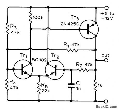
capacitor circuit operates at very low duty cycles, in range of 10% to 1%. Battery drain is low because off current is about 1 μA for 50-mA on current. R4 and C determine on time, while R1 and C set off time. Circuit pulses about twice per second, which is suitable for animal temperature and heart-rate studies. Can be used with implanted transmitters operating from single mercury button cell for more than one year with suitable resistor values.-C. Horwitz, Tolerant Astable Circuits, Wireless World, Feb. 1975, p 93. (View)
View full Circuit Diagram | Comments | Reading(667)
CRYSTAL_WITH_NOR_GATES
Published:2009/7/1 19:52:00 Author:May
Uses two sections of CD4001 quad NOR gate to give mono multivibrator operating in frequency range from 10 kHz up to top limit of about 10 MHz, with exact frequency depending on values used for R and C.-W. J. Prudhomme, CMOS Oscillators, 73 Magazine, July 1977, p 60-63. (View)
View full Circuit Diagram | Comments | Reading(890)
DIGIT_SHIFTER_FOR_DISPLAY
Published:2009/7/1 19:50:00 Author:May
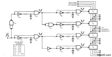
Circuit takes BCD output from 10-key keyboard and shifts each number, as entered, from right to Ieft on display panel. Intemal clock is not used. Keyboard strobe is delayed 2 ms to allow Ume for keyboard switches to stop bouncing. BCD outputs from G5-G8, go directly to 7- or 10-segment decoder driver, such as SN7447 decoders driv-ing RCA DR-2100 series low-voltage readouts.All resistors are 220 ohms. Capacitors for G1B and G1D are 1000 pF,and capacitors for othergates are 240 pF Article traces circuit operation,-T .O'Toole,Transfer Paranel Information Without a clock,EDN Magazine, Aug.1,1972,p 59. (View)
View full Circuit Diagram | Comments | Reading(725)
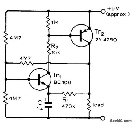
BICYCLE_SPEED_ALARM
Published:2009/7/1 19:50:00 Author:May

Useful for long-distance bicycling, to indicate when rider drops below predetermined minimum speed. Speed sensor is reed switch attached to frame and tripped once per revolution by permanent magnet mounted on wheel. Rate at which switch closes determines level of DC voltage produced by circuit. When voltage drops below preset level determined by 100K pot, output transistor comei on and energizes relay controlling bicycle hom or other signaling device. Supply can by 9-V transistor battery. Transistor reading should be high enough to handle relay used.-J. Sandler, 9 Projects under $9, Modem Electronics, Sept, 1978, p 35-39. (View)
View full Circuit Diagram | Comments | Reading(1179)
DUAL_EDGE_TRIGGERING
Published:2009/7/1 19:49:00 Author:May
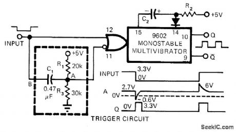
Although 9602 multivibrator IC can be triggered normally either on leading or falling edge of square wave, but not on both, addition of two resistors and one capacitor provides double-edge triggering. When input goes low, negative-going pulse through C1 triggers 9602 and makes it deliver one output pulse. When input goes high again, high-going pulse is delivered directly to pin 12 of 9602, triggering it again so it produces an other pulse.-J. P. Yang, Circuit Triggers 0ne-Shot on Both Edges of Square Wave, EDN Magazine, Nov. 15, 1972, p 49. (View)
View full Circuit Diagram | Comments | Reading(560)
BINARY_LINE_STATES
Published:2009/7/1 19:46:00 Author:May
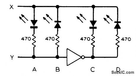
Simple circuit using four LEDs and one inverter (which may be a transistor or spare gate) displays all four possible states on two binary tines. When levels of lines X and Y are the same, A and B will be off.Inverter then places C and D at different levels so one LED (C or D) will be on, Reverse situation occurs when X and Y are at different levels.-D.Straker, Binary State Indicator, Wireless World, Feb. 1977, p 44. (View)
View full Circuit Diagram | Comments | Reading(527)
TIMER_DRIVES_LED_DlSPLAY
Published:2009/7/1 19:44:00 Author:May

Intersil 7227 microprocesso-rcontrolled timer provides direct drive for LED display under supervision of microprocessor. Tristate 4-bit data bus serves to read in control word such as up/down, store reset, or load, then deliver counter data, feed in settable register word, or preset counter to initial value.-B. O'Neil, IC Timers-the Old Reliable 555 Has Company, EDN Magazine, Sept.5, 1977, p 89-93. (View)
View full Circuit Diagram | Comments | Reading(1212)
LOW_POWER_TTL_MONO
Published:2009/7/1 5:41:00 Author:May
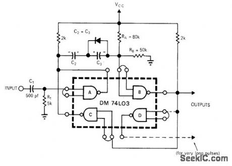
Simple monostable circuit using DM74L03 draws only 800-μA standby current yet delivers pulses up to 1 s wide. Uses RC time control and regenerative feedback, with values of C2 and C3 determining frequency. Pulse width increases from 0.1 s to 0.55 s as C2 and C3 are increased from 10μF to 60 μF.-C. Gilbert and C. Davis, LPTTL One-Shot Yields Wide, Clean Pulses, EDNIEEE Magazine, May 15, 1971, p 47-48. (View)
View full Circuit Diagram | Comments | Reading(630)
DIPPER_
Published:2009/7/1 5:41:00 Author:May
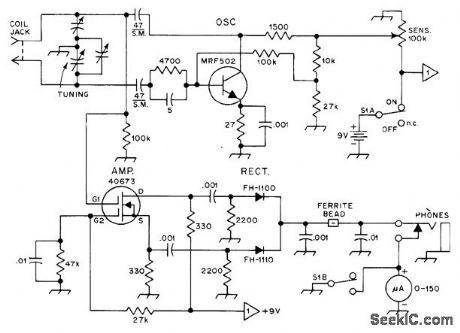
Circuit of Heath HD-1250 solid-statedlρ meter covers 1.6-250 MHz range with six plug-in coils.-The Heath HD-1250 Diρ Meter,QST, Jan 1976,p 38-39. (View)
View full Circuit Diagram | Comments | Reading(896)
6_DIGIT_LED_DRIVER
Published:2009/7/1 5:39:00 Author:May

National DS8877 drive is shown in configuration for use with 6-digit calculator Digit current is in range of 5-50 mA,Driver requires no standby power and operates from either 4.5 V, 6 V, or 9 V.- Interface Databook National Semiconductor,Santa Clara,CA,1978, p 5-52-5-53. (View)
View full Circuit Diagram | Comments | Reading(774)
LED_BRIGHTNESS_CONTROL_1
Published:2009/7/1 5:38:00 Author:May
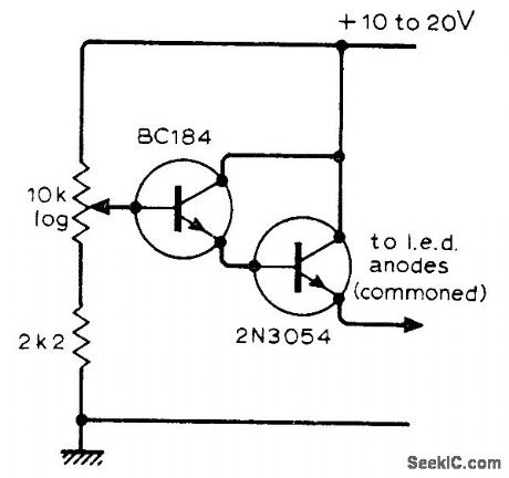
Uses 10K logarithmic pot to vary brightness simultaneously for all LEDs in digital display.-S.F.Bywatelsand J,E West,Peak-Reading Audio Level Indicator,Wireless World, Aug. 1975,p 357-36. (View)
View full Circuit Diagram | Comments | Reading(665)
| Pages:1178/2234 At 2011611162116311641165116611671168116911701171117211731174117511761177117811791180Under 20 |
Circuit Categories
power supply circuit
Amplifier Circuit
Basic Circuit
LED and Light Circuit
Sensor Circuit
Signal Processing
Electrical Equipment Circuit
Control Circuit
Remote Control Circuit
A/D-D/A Converter Circuit
Audio Circuit
Measuring and Test Circuit
Communication Circuit
Computer-Related Circuit
555 Circuit
Automotive Circuit
Repairing Circuit