
Circuit Diagram
Index 1176
SCANNER_SWEEP_FAILURE_ALARM
Published:2009/7/24 3:33:00 Author:Jessie


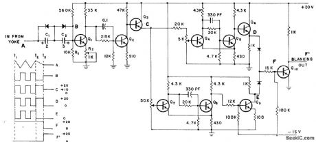
Prevents burning of phosphor on face of flying-spot stunner if sweep is lost. Consists of differentiator-amplifier, high and low-level detector, inverter, and summing and blanking generator. All transistors are 2N1302, and all diodes are 1N497.-Flying Spot Scanner Sweep Alarm, Electronic Circuit Design Handbook, Mactier Pub. Corp., N.Y., 1965, p 125. (View)
View full Circuit Diagram | Comments | Reading(685)
150_MHz_5_W_MOS_amplifier_28_V_supply
Published:2009/7/24 3:32:00 Author:Jessie
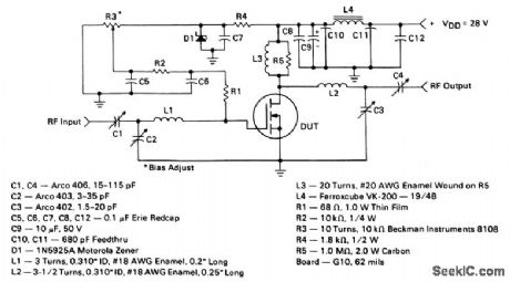
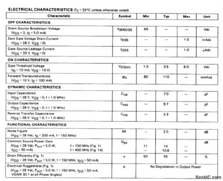
The electrical characteristics for the MRF134 shown in this circuit are given in Fig. 2-46B. (View)
View full Circuit Diagram | Comments | Reading(616)
CONSTANT_AMPLITUDE_FOR_THREE_RANGES
Published:2009/7/24 3:32:00 Author:Jessie

Multiple-range sweep generator for airborne radar provides constant-amplitude out put sawtooth, along with fast-rising gate pulse or pedestal having duration of saw tooth. linearity is kept within 1% without using bootstrap.-H. P. Brockman, Sweep Generator Design: How to Keep It Simple, Electronics, 33:3, p 92. (View)
View full Circuit Diagram | Comments | Reading(784)
HETERODYNE_FREQUENCY_METER_
Published:2009/7/1 20:18:00 Author:May

Circuit consists of 1-2 MHz oscillator Q1, untuned mixer X1, and AF beat-note amplifier Q2. C4 is calibrated to read directly in frequency from 1 to 2 MHz, using accurate unmodulated RF signalgenerator. After calibration, unknown RF signal input frequency is fed into meter for zero-beating with harmonics of calibrated oscillator.Magnetic headphones plugged into J1 make beat note audible. On second harmonic, dial of C4 covers 2-4 MHz; on twentieth harmonic, coverage is 20-.40 MHz. L1 is 65 tums No. 28 enamel on 1-inch form, tapped 20 tums from ground. L2 is 10 tums No. 28 enamel closewound around center of L1.-R. P. Turner, FET Circuits, Howard W. Sams, Indianapolis, IN, 1977, 2nd Ed., p 144-146. (View)
View full Circuit Diagram | Comments | Reading(915)
Level_transducer_digitizer
Published:2009/7/24 3:32:00 Author:Jessie
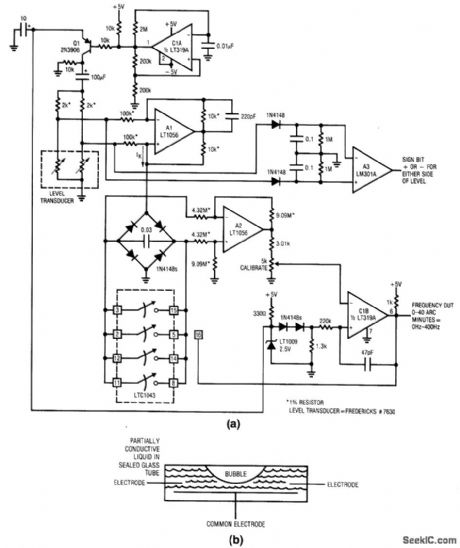
Fig.14-7 This circuit converts the angle(from an ideal level)to a corresponding frequency using a simple bubble-based transducer such as shown in Fig 14-7B.The circuit also provides a sign output(+ or -)to show either side of ideal level.If the transducer (bubble tube) is level with respect to gravity, the bubble is at the tube center and the electrode resistances to common are identical. As the tube shifts away from level, the resistances increase and decrease proportionally. By controlling the tube shape at manufacture, it is possible to get a linear output signal when the transducer is incorporated into a bridge circuit. To calibrate, place the level transducer at a known 40 arc-minute angle and adjust the calibrate potentiometer (at C1B) for a 400-Hz output. Circuit accuracy is limited by the transducer to about L5% Linear Technology Linear Applications Handbook l990, p. ANl7-12, -23. (View)
View full Circuit Diagram | Comments | Reading(609)
LOW_BATTERY_DRAIN
Published:2009/7/1 20:18:00 Author:May

Combination of astable and bistable MVBRs, connected so diagonally opposite transistors switch on and off together, minimizes current drain in battery-powered signal generator. Period of square wave is approximately equal to 1.4CR, and peak load current can be up to 70 mA with 24-V battery supply. Circuit will tolerate wide range of values for CB.-J. C. Hopkins, Efficient Square-Wave Oscillator, Wireless World, June 1977, p 58. (View)
View full Circuit Diagram | Comments | Reading(643)
SCA_DECODER
Published:2009/7/1 20:17:00 Author:May

The circuit uses a Signetics NE565 PLL (Phase-Locked Loop) as a detector to recover the SCA signal. The input to the SCA decoder circuit is connected to an FM receiver at a point between the FM discriminator and the de-emphasis filter network. The PLL, IC1, is tuned to 67 kHz by R7, a 5 K potentiometer. Tuning need not be exact since the circuit will seek and lock onto the subcarrier. The demodulated signal from the FM receiver is fed to the input of the 565 through a high-pass filter consisting of two 510 pF capacitors (C1 and C2) and a 4.7 K resistor (R1). Its purpose is to serve as a coupling network and to attenuate some of the main channel spill. The demodulated SCA signal at pin 7 passes through a three-stage de-emphasis network as shown. The resulting signal is around 50 mV, with the response extending to around 7 kHz. (View)
View full Circuit Diagram | Comments | Reading(2596)
DUTY_CYCLE_CONTROL
Published:2009/7/1 20:17:00 Author:May
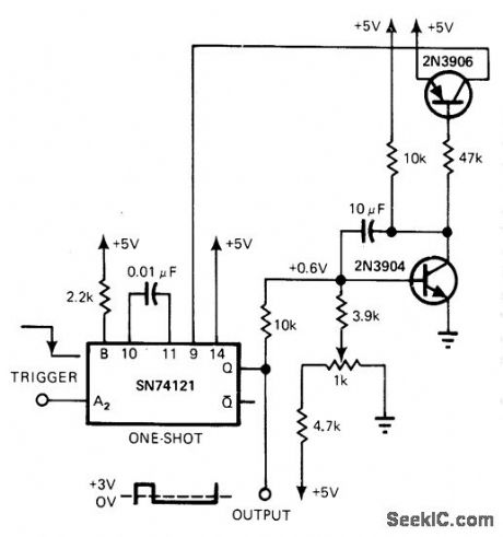
Feedback loop through two transistors automatically adjusts timing of MVBR to hold duty cycle constant over wide range of triggering rates. 2N3904 acts as integrator with time constant much longer than pulsing period. If duty cycle increases or decreases, current into integrator becomes positive or negative and DC voltage at its collector slowly decreases or increases. This collector voltage drives 2N3906 operating as current generator for adjusting automatically to give chosen duty cycle as selected by 1K pot. Range is 17% to above 50%.-J. L. Engle, Regulate Duty Cycle Automatically, EDN Magazine, Nov, 5, 1978, p 122. (View)
View full Circuit Diagram | Comments | Reading(856)
CMOS_DRIVE_FOR_LCD
Published:2009/7/1 20:16:00 Author:May

Seven-segment Iiquiocrystal display digit can be driven directly by CD4054A, CD4055A,or CD4056A CMOS because these circuits contain internal leve-shifting feature needed to convert 5-V input logic swings to 30-V peak AC sigpal required for driving dynamic-scattering LCD,- COS/MOS Integrated Circuits, RCA Solid State Dlvision,Somerville,NJ,1977,p 629. (View)
View full Circuit Diagram | Comments | Reading(1459)
NEGATIVE_GOING_DUAL_OUTPUT_555
Published:2009/7/1 20:16:00 Author:May
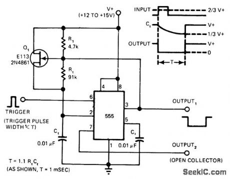
Circuit triggers on positive-going pulses and delivers negative-going output timing pulses. C1 charges when JFET switch a, is held on by high output state of timer. When output of timer goes low, Ct discharges to ground through Rt. Timing accuracy is good, and duty cycles above 99% are possible without jitter.-W. G. Jung, Take a Fresh Look at New IC Timer Applications, EDN Magazine, March 20, 1977, p 127-135. (View)
View full Circuit Diagram | Comments | Reading(1019)
DIRECT_COUPLED_ASTABLE
Published:2009/7/1 20:14:00 Author:May
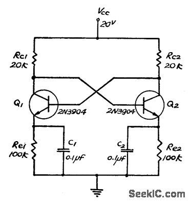
Collectors and bases of both emitter-biased transistors are directly coupled to each other. Switching action takes place by means of capacitor in each emitter circuit. Triangle waves are generated at emitters. Neither transistor can remain permanently cut off. Instead, circuit has two quasi-states, with switching action achieved by charging and discharging capacitor between these states. Single 0.1-μF capacitor can be used between emitters in place of C1 and C2.-S. Chang, Two New Direct-Coupled Astable Multivibrators, Proceedings of the IEEE, March 1973, p 390-391. (View)
View full Circuit Diagram | Comments | Reading(543)
Sampled_strain_gauge_conditioner
Published:2009/7/24 3:42:00 Author:Jessie
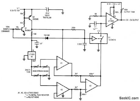
Fig, 14-13 This circuit converts the output of a strain-gauge to a corresponding voltage, but with considerable power savings produced by sampling. An external 10-Hz sampling signal or command is required. Effective current drain is about 300μA, and the A4 output is accurate enough for 12-bit systems. The 100-kΩ output trim pot is suitable for 3 mV/V transducers, but it might require a different value for other transducers, Linear Technology Linear Applications Handbook, 1990 AN23-3. (View)
View full Circuit Diagram | Comments | Reading(681)
CLOCK_SYNCHRONIZED
Published:2009/7/1 20:14:00 Author:May
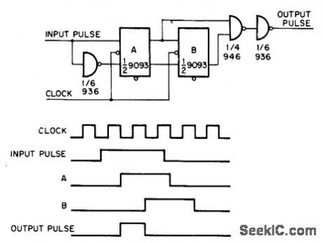
Circuit generates pulse that is two clock pulses wide, in synchronism with clock, from random input pulse whose width is more than 5 times that of clock pulse.
Flip-flops A and B are connected as shift register. When clock pulse falls, input of flip-flop A goes to 1 and sets it. B follows state of A with delay of one clock pulse. Output pulse can occur only once during a particular input strobe.-F. E. Nesbitt, Synchronized One Shot, EDN|EEE Magazine, May 15, 1971, p 50. (View)
View full Circuit Diagram | Comments | Reading(695)
GATED_PULSE_DESCRAMBLER
Published:2009/7/1 20:13:00 Author:May
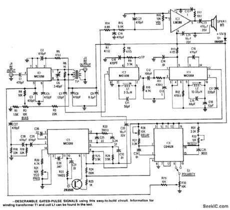
This circuit consists of an amplifier and video detector with a second subcarrier detector for synch recovery purposes. A pulse-former circuit modulates the gain of the main channel increasing it during synch intervals. Provision for subcarrier audio descrambling is also provided. Kit available from North Country Radio, P.O. Box 53, Wykagyl Station, New York 10804. (View)
View full Circuit Diagram | Comments | Reading(1531)
TRIODE_PHANTASTRON_SWEEP
Published:2009/7/24 3:42:00 Author:Jessie

Active elements V1-V2 serve with isolation diode V3 to give action of single pentode with good sweep linearity.-A. S. Kislovsky, Sweep Circuits Using Two Three-Terminal Active Elements, Electronics, 35:12, p 54-55. (View)
View full Circuit Diagram | Comments | Reading(615)
17_Hz_SQUARE_WAVES
Published:2009/7/1 20:13:00 Author:May
Uses three comparators from MC3302P IC to generate three sym-metrical square waves 120° apart. Inverting out-puts of comparators gives waves 60° apart. Operating voltage can be anywhere from 4 to 12V.-L,J. Bell, Three Coupled Astables, Wire-less World, Feb. 1977, p 44. (View)
View full Circuit Diagram | Comments | Reading(472)
Micropower_voltage_reference
Published:2009/7/24 3:42:00 Author:Jessie

This circuit provides an adjustable voltage reference with a temperature coefficient of 0.002%/°C, and an overall standby current of less than 100 μA, using the zero-temperature-coefficient characteristic of a JFET (J1 is biased slightly below pinchoff by P1). (View)
View full Circuit Diagram | Comments | Reading(747)
PERFECT_SOUARE_WAVES_FORLAB
Published:2009/7/1 20:12:00 Author:May
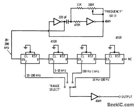
Two sections of 4049 hex inverting buffer are connected as 10:1 variable-frequency astable MVBR to feed chain of four divide-by-10 counters using 4518 dual counters. Frequency division pro-vides perfect symmetry for square-wave out-put.-D. Lancaster, CMOS Cookbook, Howard W. Sams, Indianapolis, IN, 1977, p 232-234. (View)
View full Circuit Diagram | Comments | Reading(715)
ASTABLE_USING_CMOS_TRANSISTOR_PAIR
Published:2009/7/1 20:12:00 Author:May
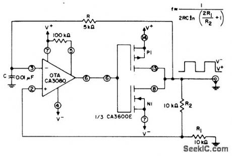
One transistor pair from CA3600E array is used with CA3080 operational transconductance amplifier to give precise timing and threshold for square waves,Quiescent power consumption is typically 6 mW with values shown.-''Linear Integrated Circuits and MOS/FET’s.''RCA Solid State Division, Somerville、NJ、1977, p 279. (View)
View full Circuit Diagram | Comments | Reading(2151)
150_MHz_30_W_PEP_MOS_amplifier_28_V_supply
Published:2009/7/24 3:41:00 Author:Jessie

The electrical characteristics for the MRF138 shown in this circuit are given in Fig.2-50B (View)
View full Circuit Diagram | Comments | Reading(525)
| Pages:1176/2234 At 2011611162116311641165116611671168116911701171117211731174117511761177117811791180Under 20 |
Circuit Categories
power supply circuit
Amplifier Circuit
Basic Circuit
LED and Light Circuit
Sensor Circuit
Signal Processing
Electrical Equipment Circuit
Control Circuit
Remote Control Circuit
A/D-D/A Converter Circuit
Audio Circuit
Measuring and Test Circuit
Communication Circuit
Computer-Related Circuit
555 Circuit
Automotive Circuit
Repairing Circuit