
Circuit Diagram
Index 1177
Pressure_transducer_conditioner
Published:2009/7/24 3:41:00 Author:Jessie
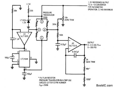
Pig. 14-12 This circuit converts the output of a pressure transducer to a voltage and it provides a 1.2-V reference output to a monitoring A/D converter for ratiometric operation (0.1 mA max/min). The circuit converts the bridge differential output into a ground-referred single-ended signal, which is then amplified. This approach eliminates common-mode errors by eliminating the bridge common-mode output component. No precision resistor matching is required. To calibrate, apply (or electrically simulate) 0 psi, and adjust the zero trim for 0-V output. Then, apply (or electrically simulate) 350 psi and adjust the gain trim for 3.500-V output. Repeat these adjustments until both points are fixed. Linear Technology Linear Applications Handbook 1990 p AN11-7.
(View)
View full Circuit Diagram | Comments | Reading(637)
SPARK_COIL_TACHOMETER_
Published:2009/7/1 20:11:00 Author:May

Input to National LM2917 tachometer IC is taken from spark-coil distributor terminal of gasoline engine. Frequency of input signal is converted to voltage for driving meter. Circuit is set up for number of cylinders on engine by adding link for appropriate timing resistor. Zener protects IC from transients found in auto battery circuit.- Linear Applications, Vol. 2, National Semiconductor, Santa Clara, CA, 1976, AN-162, p 9-10. (View)
View full Circuit Diagram | Comments | Reading(1104)
FREE_RUNNING_GROUNDED_GRID
Published:2009/7/24 3:41:00 Author:Jessie

Has higher output impedance than other time-base sweep circuits. Reducing RL increases period.-C. Sing, Grounded-Grid Circuit Sweeps Better Than Miller or Bootstrap, Electronics, 38:6, p 83-84. (View)
View full Circuit Diagram | Comments | Reading(642)
BASIC_MONO
Published:2009/7/1 20:11:00 Author:May
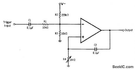
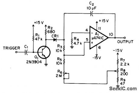
Opamp is normally in positive saturation because of negative voltage pro-vided by voltage divider R2-R3. When 2-V positive trigger pulse is applied to input, output of opamp swings into negative saturation but automatically returns to positive saturation after time interval determined by values used for C2 and R4. With R4 set at maximum resistance, this time is about 1 s. Increase size of C2 for longer time periods. Opamp can be 741 or equivalent.-R. Melen and H. Garland, Under-standing IC Operational Amplifiers, Howard W. Sams, Indianapolis, IN, 2nd Ed., 1978, p 120-121. (View)
View full Circuit Diagram | Comments | Reading(642)
MONO_WITH_NORMALLY_ONLED
Published:2009/7/1 20:10:00 Author:May
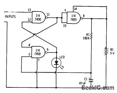
Connection shown for three gates of 7400 quad NAND gate inverts operating mode, so LED is normally on. Trigger pulse at input extinguishes LED for time determined by R1 and C1 while making gates change states. Gates revert to original states after delay also determined by values of R1 and C1.-F. M. Mims, Integrated Circuit Projects, Vol. 2, Radio Shack, Fort Worth, TX, 1977, 2nd Ed., p 19-26. (View)
View full Circuit Diagram | Comments | Reading(580)
Low_voltage_step_up_converter_with_higher_power_output
Published:2009/7/24 3:41:00 Author:Jessie

This circuit is similar to that of Fig. 8-42, except that an N-channel FET is added to provide 250 mA output current. (View)
View full Circuit Diagram | Comments | Reading(683)
IC_FLIP_FLOP_DEMONSTRATOR
Published:2009/7/1 20:09:00 Author:May

Demonstration circuit using RS7473 dual flip-flop incorporates 555 clock circuit providing sequential train of input pulses at AF rate to JK master slave flip-flop section for toggling LED loads of flip-flop back and forth between ON and OFF states. R1 controls rate at which LEDs flash on and off. Circuit is designed for Radio Shack 276041 or equivalent red LEDs. If clock is omitted, state of flip-flop is changed by grounding clock input pin 1 momentarily.-F. M. Mims, Integrated Circuit Projects, Vol. 6, Radio Shack, Fort Worth, TX, 1977, p 23-32. (View)
View full Circuit Diagram | Comments | Reading(5918)
FAST_RESET_SAWTOOTH
Published:2009/7/24 3:41:00 Author:Jessie

Regenerative pnp npn pctir in positive-feedback circuit Q1 is constant-current charging source for C1, with R2 varying charging rate and free-running frequency, which can range from 60 cps to 1 Mc.-N. C. Hekimian, PNP.NPN CIRCUITS: New Look at a Familiar Connection, Electronics, 35:47, p 42-46. (View)
View full Circuit Diagram | Comments | Reading(645)
DARLINGTON_WITH_BOOTSTRAP_FLIP_FLOP_SWEEP
Published:2009/7/24 3:40:00 Author:Jessie

Transistor Q3 in Darlington con nection improves linearity of controllable sweep comparable to vacuum-tube phantostron.-J. B. Payne III, Voltage-Controlled Bootstrap Generator, Electronics, 33:11, p 177-178. (View)
View full Circuit Diagram | Comments | Reading(796)
TRIGGERED_MVBR
Published:2009/7/1 20:08:00 Author:May
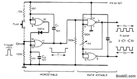
Each trigger input produces fixed number of pulses, between 2 and 30 depending on setting of 1-megohm frequency control. Monostable feeds gated astable, both realized with single CD4001 IC. Use dashed circuit with pushbutton for manual operation in place of trigger pulse.-K, Padmanabhan, N-Stable Multivibrator, Wireless World, April 1977, p 61. (View)
View full Circuit Diagram | Comments | Reading(1157)
Micropower_voltage_regulator
Published:2009/7/24 3:40:00 Author:Jessie

Figure 8-4 shows a MAX663 connected to provide a+5-V output at 40 mA from a 9-V battery. The maxlmum quiescent currentis 12 μA.MAXIM NEW RELEASES DATABook 1992. P.4-125. (View)
View full Circuit Diagram | Comments | Reading(726)
RETRIGGERABLE_MONO
Published:2009/7/1 20:07:00 Author:May
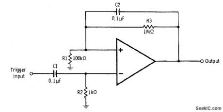
Circuit provides pulse widths up to 60 s, has short reset time, and can be retriggered during timing cycle. Pulse width is determined by C2, R3, R5, and R6.If trigger pulse arrives while output of A1 is high, C2 discharges to its original triggered state for initiating completely new timing cycle.-D. Pantic, Retriggerable Monostable, EDN|EEE Magazine, May 15, 1971, p 50. (View)
View full Circuit Diagram | Comments | Reading(613)
Strain_gauge_conditioner_digitizer
Published:2009/7/24 3:40:00 Author:Jessie

Fig. 14-11 This circuit converts the dc output of a classic strain-gauge transducer to a frequency (actually a ratio of two frequencies). For a typical 7.5-μV strain-gauge bridge drive, an LSB increment is 25 μV (below most conventional A/D converters). The circuit data output (the ratio of output A to the clock frequency) can be extracted with counters. Because the output is expressed as a ratio, clock-frequency stability is unimportant. However, careful layout and a clean PC board are required. Use a teflon standoff for all summing-point connections. If a particular strain-gauge transducer requires zero trimming, use the optional network. Over a 0 to 70℃ range, the circuit typically maintains a 10-bit output with 1 LSB accuracy. The tracking error of the starred resistors are the primary contributors to this small error. No calibration is required. Linear Technology Linear Applications Handbook, 1990. p AN7-6. (View)
View full Circuit Diagram | Comments | Reading(1735)
TIMING_PULSE_GENERATOR
Published:2009/7/1 20:06:00 Author:May
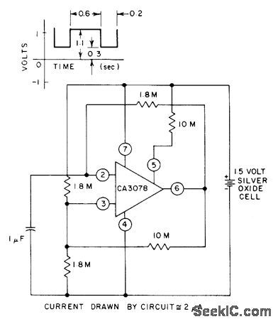
Astable MVBR uses CA3078 micropower opamp to develop timing pulses for driving other low-power circuits. Current drain is only about 2μA from 1.5-VDC supply.- Circuit ideas for RCA Linear ICs, RCA Solid State Division, Somerville, NJ, 1977, p 4. (View)
View full Circuit Diagram | Comments | Reading(692)
2_to_50_MHZ_30_W_PEP_MOS_amplifier_28_V_supply
Published:2009/7/24 3:39:00 Author:Jessie
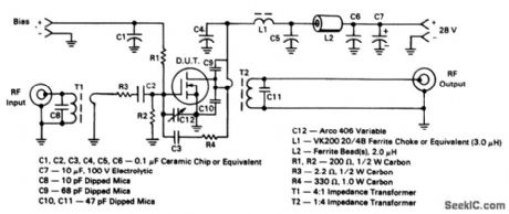
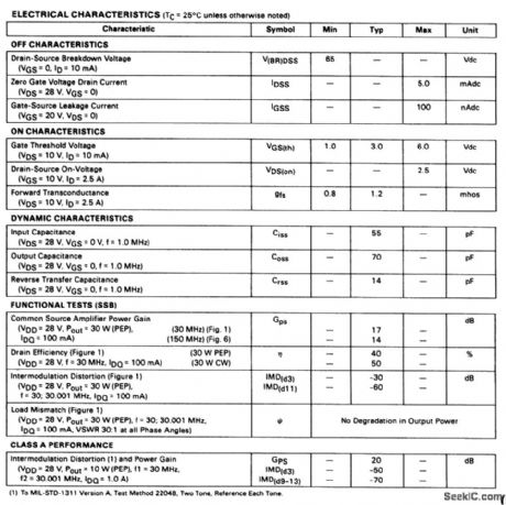
The electrical characteristics for the MRF138 shown in this circuit are given in Fig 2-50B (View)
View full Circuit Diagram | Comments | Reading(887)
0_10kHz_to_0_10VDC_
Published:2009/7/1 20:06:00 Author:May

Raytheon 4151VFC voltage-to-frequency converter is used in reverse as linear frequency-to-voltage converter.Applications include use in pairs as complete data transmission system, for remote monitoring of DC voltage such as output of SWR bridge located at junction of antenna with transmission line. DC voltage is changed into audio volt-age at remote location, sent over lines, then changed back to DC at readout location. Line characteristics do not affect frequency of audio signal.-J. J. Schultz, A Voltage-to-Frequency Converter IC with Amateur Applications, CQ, Jan. 1977, p 39-41 and 75. (View)
View full Circuit Diagram | Comments | Reading(2137)
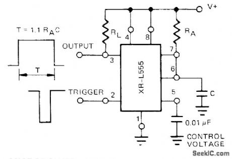
BASIC_555_MONO
Published:2009/7/1 20:06:00 Author:May

Circuit variation shown for original IC timer prototype has same timing equation and input trigger requirements for standard connection but provides two outputs rather than one. This is achieved by using pin 7 of IC as an open-collector output that can be referred to any supply voltage between 0 and +15 V regardless of voltage used for timer. Article describes operation in detail and points out possible drawbacks, including possibility of timing error for high duty cycle operation because C1 takes longer to discharge than in conventional monostable MVBR -W G. Jung, Take a Fresh Look at New IC Timer Applications, EDN Magazine, March 20, 1977, p 127-135. (View)
View full Circuit Diagram | Comments | Reading(900)
AC_COUPLED_FLIP_FLOP
Published:2009/7/1 20:05:00 Author:May
When leading edge of 2-V positive trigger pulse is applied to negative input of 741 or equivalent opamp, this input becomes more positive than positive input and opamp swings into negative saturation. This condition is held by positive feedback until trailing edge of next trigger pulse makes opamp swing back into positive saturation. C2 prevents trailing edge of first pulse from driving opamp back into positive saturation. Value shown for C2 should be increased if pulses are longer than 50 ms.-R. Melon and H. Garland, Understanding IC Operational Amplifiers, Howard W. Sams, Indianapolis, IN, 2nd Ed., 1978, p 118-119. (View)
View full Circuit Diagram | Comments | Reading(904)
MICROPOWER_CLOCK
Published:2009/7/1 20:04:00 Author:May
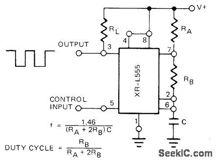

Free-running frequency and duty cycle are controlled by RA, RB, and C in astable MVBR connection of Exar XRL555 micropower equivalent of 555 timer. With 5-V supply, power dissipation is only 900μW.- Timer Data Book, Exar Integrated Systems, Sunnyvale, CA 1978 p 7-8. (View)
View full Circuit Diagram | Comments | Reading(875)
DIVIDING_FOR_SYMMETRY
Published:2009/7/1 20:03:00 Author:May
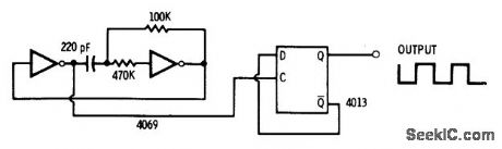
4013 dual D flip-flop is used as binary divider at output of astable MVBR to give 50/50 symmetry for output frequency half that of MVBR.-D. Lancaster, CMOS Cookbook, Howard VV. Sams, Indianapolis, IN, 1977, p 232-234. (View)
View full Circuit Diagram | Comments | Reading(591)
| Pages:1177/2234 At 2011611162116311641165116611671168116911701171117211731174117511761177117811791180Under 20 |
Circuit Categories
power supply circuit
Amplifier Circuit
Basic Circuit
LED and Light Circuit
Sensor Circuit
Signal Processing
Electrical Equipment Circuit
Control Circuit
Remote Control Circuit
A/D-D/A Converter Circuit
Audio Circuit
Measuring and Test Circuit
Communication Circuit
Computer-Related Circuit
555 Circuit
Automotive Circuit
Repairing Circuit