
Circuit Diagram
Index 1175
FET_REDUCES_PREAMP_NOISE
Published:2009/7/24 4:33:00 Author:Jessie
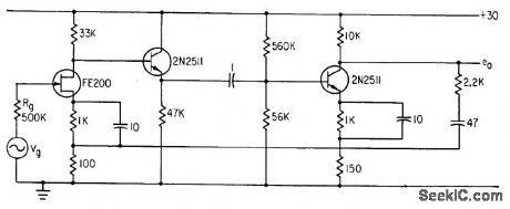
When impedance of source Vg is high, field-effect transistors reduce overall signal-to-noise folio in preamp for reproduce head of tope re corder.-J. J. Rado, Designing Input Circuits with Lowest Possible Noise, Electronics, 36:31, p 46-49. (View)
View full Circuit Diagram | Comments | Reading(739)
STEREO_TV_DECODER
Published:2009/7/1 20:28:00 Author:May

The composite input signal is preamplified by transistor Q1 and is then coupled to the high-pass filter composed of C3, C4, R6, and R7. The filtered audio is then passed to IC1, an MC1310P Coilless Stereo Demodulator. That IC is normally used to demodulate broadcast-band FM signals, but by changing the frequency of its on-board VCO (Voltage Controlled Oscillator) slightly (from 19 kHz to 15.734 kHz), we can use that IC to detect stereo-TV signals. A block diagram of the MC1310P is shown in Fig.22-5. Notice that the components connected to pin 14 control the VCO's frequency, hence the pilot-detect and carrier frequencies. For use in an FM receiver, the VCO would run at four times the 19 kHz pilot frequency (76 kHz), but for our application, it will run at four times the 15.734 kHz pilot frequency of stereo TV, or 62.936 kHz. The MC1310P divides the master VCO signal by two in order to supply the 31.468 kHz carrier that is used to detect the L - R audio signal. The L - R signal undergoes normal FM detection, and at that point we've got two audio signals: L + R and L - R. The decoder block in the IC performs the addition and subtraction to produce the separate left and right signals. R10and C10 form a de-emphasis network that compensates for the 75μs pre-emphasis that the left channel underwent; R12 and C11 perform the same function for the right channel. (View)
View full Circuit Diagram | Comments | Reading(0)
4_DIGIT_DIRECT_DRIVE_LCD
Published:2009/7/1 20:27:00 Author:May

Each digit of liquid crystal display has sepalate counter,latch,decoder,and driver,Excitation signal also feeds LCD backplane When segmentis to be deenergized, backplane and segment drive signals have same phase and magnitude so there is no voltage across display. When segment is to be energized, signals are 180°out of phase so square-wave voltage is twice IC supply value.BCD inputs are generated from cascaded MC14518 dual BCD up counters.-A. Pshaenich, Interface Considerations for Numeric Display Systems, Motorola, Phoenix, AZ, 1975, AN-741,p 5. (View)
View full Circuit Diagram | Comments | Reading(2310)
HIGH_PRECISION_F_V
Published:2009/7/1 20:26:00 Author:May
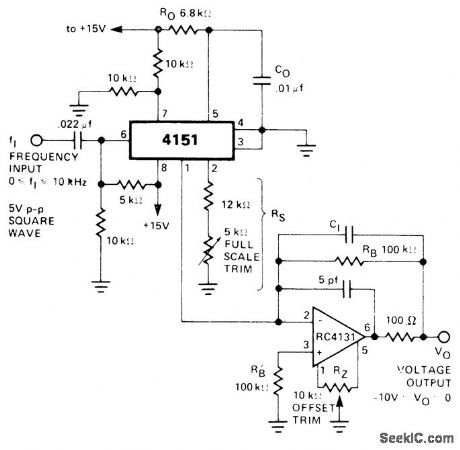
Use of integrator opamp with frequency-to-voltag e connection of RM4151 converter gives increased accuracyand linearity for converting square-wave inputs of 0-10 kHz to proportional output voltage in range of -10 V to 0 V.- Linear Integrated Circult Data Book, Raytheon Semiconductor Division, Mountain View, CA, 1978, p 7-39. (View)
View full Circuit Diagram | Comments | Reading(523)
VOLTAGE_CONTROLLED_MONO_1
Published:2009/7/1 20:25:00 Author:May

Circuit gives choice of Linear sawtooth and constant pulse-width outputs over frequency range from DC to 50 kHz. Output frequency and pulse repetition rate vary linearly with control current. Applications include audio synthesizers, variable time bases, and current-to-frequency converters.-S. Wetenkamp, Minor Changes Turn VCO into Voltage-Controlled One-Shot, EDN Magazine, March S, 1978, p 67-69. (View)
View full Circuit Diagram | Comments | Reading(1957)
8_DIGIT_LED_DRIVE
Published:2009/7/1 20:25:00 Author:May

National DM8863 8-digit LED driver is used Inconjunction with DM75491 and DM8861 drivers for driving eight commonmode LED digits operating in multiplex mode.Circuit also provides logic control for decimal point.-C Carinalli, Driving 7-Segment LED Displays with National Semiconductor Circults, National Semiconductor,Santa Clara,CA,1974,AN-99,p 10. (View)
View full Circuit Diagram | Comments | Reading(587)
MOSFET_ASTABLE
Published:2009/7/1 20:24:00 Author:May
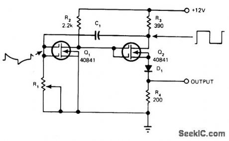
RCA 40841 dual-gate N-channel depletion-type MOSFETs alternate between high and low conduction states in between dormant periods when C1 is charging or discharging through R1 Circuit switches state when voltage level at gate of a, makes gain lf high enough for regeneration to occur. D1 reduces voltage across R4 to give TTL drive capability.-D. R. Armstrong, Wide-Frequency Astable Multivibrator Uses One R-C Network, EDN Magazine, Aug, 5, 1977, p 54. (View)
View full Circuit Diagram | Comments | Reading(2196)
UJT_MONO
Published:2009/7/1 20:23:00 Author:May
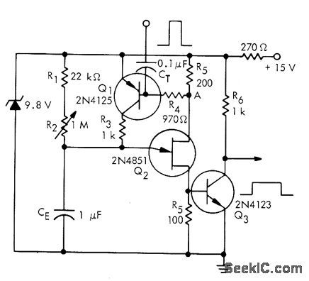
UJT Q2 is normally on, with its emitter saturation current supplied by transistor Q1 which is also on. Application of positive trigger pulse to base of a, turns both off to start timing cycle. CE starts charging each time from saturation voltage of UJT. When capacitor voltage becomes high enough to fire UJT, Q1 turns on and supplies emitter current required to keep UJT on. Output transistor a, delivers pulse having duration related to value used for CE.- Unijunction Transistor Timers and Oscillators, Motorola, Phoenix, AZ, 1974, AN-294 p 5. (View)
View full Circuit Diagram | Comments | Reading(723)
DUAL_TIME_CONSTANT_TONE_DECODER
Published:2009/7/1 20:22:00 Author:May


For some applications it is important to have a tone decoder with narrow bandwidth and fast response time. This can be accomplished by the dual time constant tone decoder circuit shown.The circuit has two low-pass loop filter capacitors, C2 and C'2. With no input signal present, the output at pin 8 is high, transistor Q1 is off, and C'2 is switched out of the circuit.Thus, the loop low-pass filter is comprised of C2, which can be kept as small as possible for minimum response time. When an in-band signal is detected, the output at pin 8 will go low, Q1 will turn on, and capacitor C'2 will be switched in parallel with capacitor C2. The low-pass fil-ter capacitance will then be C2 + C'2. The val-ue of C'2 can be quite large in order to achieve narrow bandwidth. During the time that no input signal is being received, the bandwidth is de-termined by capacitor C2. (View)
View full Circuit Diagram | Comments | Reading(0)
10_W_CW_TRANSCEIVER_POWER_SUPPLY
Published:2009/7/24 3:34:00 Author:Jessie

This power supply delivers about 24 Vdc at 1 A and was originally used for supplying power to a 10-W CW ham rig. (View)
View full Circuit Diagram | Comments | Reading(482)
TRANSISTORS_SIMULATE_PHANTASTRON
Published:2009/7/24 3:34:00 Author:Jessie

Three transistors simulate current-partitioning action of pentode vacuum-tube phantastron sawtooth sweep generator. Potentiometer in bias and feedback circuit can be adjosted for either triggered or free-running phantastron sweep.-N. C. Hekimian, Phantastron Circuits Using Transistors, Electronics, 34:8, p 46-47. (View)
View full Circuit Diagram | Comments | Reading(621)
KLYSTRON_SWEEP
Published:2009/7/24 3:34:00 Author:Jessie

Provides sweep voltage for klystron in microwave interferometer system, plus vertical sweep end trigger for oscilloscope.-H. L. Bunn, Determining Electron Density und Distribution in Plasmas, Electronics, 34:14, p 71-75. (View)
View full Circuit Diagram | Comments | Reading(868)
400_MHz_50_-W_MOS_amplifier28_V_supply
Published:2009/7/24 3:34:00 Author:Jessie
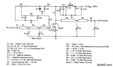
The electrical characteristics for the MRF134 shown in this circuit are given in Fig. 2-46B. Those not familiar with microstrip techniques(for Z1-Z5) should read the many Motorola publications,such as AN548A and AN555. (View)
View full Circuit Diagram | Comments | Reading(862)
Photodiode_signal_conditioner_voltage_output
Published:2009/7/24 3:34:00 Author:Jessie
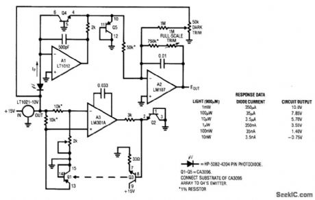
Fig. 14-8 This circuit converts the output of a PIN photodiode to a corresponding voltage. The specified photodiode responds linearly to light intensity over a 100-dB range. To accommodate this wide range without digitizing (this would require an A/D with 17 bits of range) the circuit compresses the photodiode output logarithmically (using the logarithmic relationship between VBE and collector current of transistors). This VBE/current relationship is temperature sensitive, and generally requires special layout of components. The circuit overcomes the layout problem because all transistors in the circuit are part of a CA3096 array. To calibrate, first set the thermal control loop by grounding the Q3 base and setting the 2-kΩ pot so that the A3 inverting input is 55 mV above the noninverting input. This places the servo setpoint at about 50℃ (assuming a 25℃ ambient). Remove the Q3 base ground and place the photodiode in a completely dark environment. Adjust the dark trim so that the A2 output is 0 V. Then, apply (or electrically simulate, using the chart) 1 mW of light (350μA of diode current) and set the full-scale trim for a 10-V output. Once adjusted, this circuit responds logarithmically to light inputs from 10 to 1 mW with an accuracy that is limited by the 1% photodiode error. Linear Technology Linear Applications Handbook 1990 p AN5-3. (View)
View full Circuit Diagram | Comments | Reading(1405)
555_TIMER_AS_FLIP_FLOP
Published:2009/7/1 20:21:00 Author:May
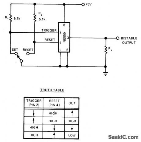
Eliminating RC timing network of 555 timer and tying threshold low makes output states depend on trigger and reset inputs. These are pulled high through R1 and R2, then pulled low either with switch or TTL level of 0 on reset input pin 4. Output then stays low until reset goes high and trigger goes low; this bistable action prevents contact bounce from switching output erroneously. Circuit will source or sink 200 mA.-R. L. Gephart, Mini-DIP Bistable Flip-Flop Sinks or Sources 200 mA, EDN Magazine, Oct. 5, 1974, p 76 and 78. (View)
View full Circuit Diagram | Comments | Reading(1241)
Simple_nanometer_microammeter
Published:2009/7/24 3:33:00 Author:Jessie

This circuit is an improved version of the circuit in Fig. 8-41, with diode input-overvoltage protection and meter-scale adjustments. Meter zero is set by R2, and full-scale deflection is set by R1 (typically, about 4 kΩ). Figure 8-41B shows the values of Rf for nanoammeter and microammeter operation. (View)
View full Circuit Diagram | Comments | Reading(2103)
12_DIGIT_GAS_DISCHARGE
Published:2009/7/1 20:21:00 Author:May

Display anodes are referenced to ground and cathodes to -180 V because number of digits in display is greater than number of segment drivers. Positive-logic CMOS address circuits are powered by -10 V, with Motorola MC14558 decoder outputs coupled to MC3491 segment drivers. Scan circuit is directly coupled to MC3490P anode drivers. Digit scanning is derived from two cascaded MC14022 octal counter/dividers. Required 12 sequenced output pulses are achieved by resetting counters with Q7 output of second counter. Counter output also controls system multiplexer (not shown) to give synchronization of entire display system.-A. Pshaenich, Interface Considerations for Numeric Display Systems, Motorola, Phoenix, AZ, 1975, AN-741, p 23. (View)
View full Circuit Diagram | Comments | Reading(890)
LOW_STANDBY_POWER
Published:2009/7/1 20:20:00 Author:May

Basic 555 timer circuit is combined with control logic to keep drain from 12-V supply down to 1μA during standby. Drain increases to 6 mA when input signal makes output pulse go high. Circuit can be interfaced with CMOS logic. Negative-going input pulse triggers SR flip-flop, which in turn saturates a, and applies power to 555. Simultaneously, C2 feeds trigger to trigger input pin 2 of 555, to make output pulse go high. At end of time delay determined by values of R and C, timer output goes low and transition resets flip-flop for standby operation.-K. J. Imhof, 555 One-Shot Circuit Features Low-Power Standby Mode, EDN Magazine, April 20, 1978, p 134. (View)
View full Circuit Diagram | Comments | Reading(1320)
100_V_output_with_shunt_regulation
Published:2009/7/24 3:33:00 Author:Jessie


Figure 7-76 shows the MAX773 connected to provide 100-V output at 10 mA, with 24-V to 28-V input. Figure 7-77 shows the calculations for selecting the RSHUNT vaLue. RSHUNT should be selected so that ISHUNT is greater than 1 mA, but less than 20 mA. If the calculated shunt regulator current exceeds 20 mA, or if the shunt current exceeds 5 mA, and less shunt-regulator current is desired, use the circuit of Fig. 7-78. This provides increased drive and reduced shunt current when driving N-FETs with large gate capacitances. Use an ISHUNT of 3 mA. This provides adequate biasing current for the circuit, although higher shunt currents can be used. Notice that the shunt regulator is not disabled in the shutdown mode, and continues to draw the calculated shunt current. To prevent the shunt regulator from drawing current in the shutdown mode, place a switch in series with the shunt resistor.See Fig. 7-68 for component suppliers. MAXIM NEW RELEASES DATA Book, 1995, P. 4-152, 4-154.
(View)
View full Circuit Diagram | Comments | Reading(836)
PRECISION_MONO
Published:2009/7/1 20:19:00 Author:May

Negative-going pulse triggers mono, making output go LOW for duration of eight clock pulses at frequency determined by values of R and C in 4011 clock generator IC1. R1 is greater than 2RT, and clock frequency is 1/13.8RTC. Width of output pulse depends on number of stages in shift register IC, and clock frequency.-B. Bong, Two CMOS IC's Yield Precision One-Shot, EDN Magazine, Aug. 5, 1978, p 82. (View)
View full Circuit Diagram | Comments | Reading(694)
| Pages:1175/2234 At 2011611162116311641165116611671168116911701171117211731174117511761177117811791180Under 20 |
Circuit Categories
power supply circuit
Amplifier Circuit
Basic Circuit
LED and Light Circuit
Sensor Circuit
Signal Processing
Electrical Equipment Circuit
Control Circuit
Remote Control Circuit
A/D-D/A Converter Circuit
Audio Circuit
Measuring and Test Circuit
Communication Circuit
Computer-Related Circuit
555 Circuit
Automotive Circuit
Repairing Circuit