Signal Processing
Photodiode_signal_conditioner_voltage_output
Published:2009/7/24 3:34:00 Author:Jessie | From:SeekIC
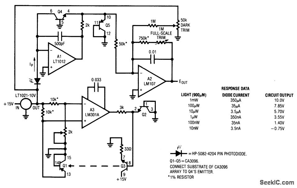
Fig. 14-8 This circuit converts the output of a PIN photodiode to a corresponding voltage. The specified photodiode responds linearly to light intensity over a 100-dB range. To accommodate this wide range without digitizing (this would require an A/D with 17 bits of range) the circuit compresses the photodiode output logarithmically (using the logarithmic relationship between VBE and collector current of transistors). This VBE/current relationship is temperature sensitive, and generally requires special layout of components. The circuit overcomes the layout problem because all transistors in the circuit are part of a CA3096 array. To calibrate, first set the thermal control loop by grounding the Q3 base and setting the 2-kΩ pot so that the A3 inverting input is 55 mV above the noninverting input. This places the servo setpoint at about 50℃ (assuming a 25℃ ambient). Remove the Q3 base ground and place the photodiode in a completely dark environment. Adjust the dark trim so that the A2 output is 0 V. Then, apply (or electrically simulate, using the chart) 1 mW of light (350μA of diode current) and set the full-scale trim for a 10-V output. Once adjusted, this circuit responds logarithmically to light inputs from 10 to 1 mW with an accuracy that is limited by the 1% photodiode error. Linear Technology Linear Applications Handbook 1990 p AN5-3.
Reprinted Url Of This Article:
http://www.seekic.com/circuit_diagram/Signal_Processing/Photodiode_signal_conditioner_voltage_output.html
Print this Page | Comments | Reading(3)

Article Categories
power supply circuit
Amplifier Circuit
Basic Circuit
LED and Light Circuit
Sensor Circuit
Signal Processing
Electrical Equipment Circuit
Control Circuit
Remote Control Circuit
A/D-D/A Converter Circuit
Audio Circuit
Measuring and Test Circuit
Communication Circuit
Computer-Related Circuit
555 Circuit
Automotive Circuit
Repairing Circuit
Code: