
Circuit Diagram
Index 1169
MULTIPLEXING_EIGHT_DlGITS
Published:2009/7/1 21:14:00 Author:May
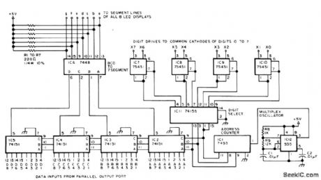
Uses only one 7-segment driver for eight digits of parallel BCD data on eight-LED display that can use MAN 4 or DL7647-segment LEDs. Power is supplied to only one digit at a time but is switched at high enough rate so all digits appear to be on. Uses one eight-channel 74151 multiplexerfor each of the 4 data input bits. Multiplexors and demultiplexer are addressed by7493 counter that is incremented at about 4 kHz by 555 oscillator.IC11 is connected for three-to eight-line demultiplexing. IC7-IC10 are peripheral interface gates, each sinking up to 300 mA for its LED.7448 decoder/driver converts BCD data to 7-segment code for driving segments of LEDs. For 74151 and 74155, pin 16 goes to +5 V and pin 8 to ground. Pin 8 of 75451 goes to +5 V and pin 4 to ground. Pin 5 of 7493 goes to +5 V and pin 10 to ground.-J. Hogenson, Multiplex Your Digital LED Displays, BYTE, March 1977, p 122-126 and 128. (View)
View full Circuit Diagram | Comments | Reading(2694)
V_F_CONVERSION_POSITIVE_INPUT_VOLTAGE
Published:2009/7/1 21:13:00 Author:May
View full Circuit Diagram | Comments | Reading(993)
10_kHz_LOW_PASS_FILTER
Published:2009/7/1 21:13:00 Author:May

Suitable for use at both input and output of A/D-D/A converter in digital audio system for synthesizing speech or music. Serves for smoothing steps of output waveform and suppressing background noise on output when small signals are being processed with 8-bit Iinear encoding.-T. Scott. Digital Audio. Kilobaud, May 1977. p 82-86. (View)
View full Circuit Diagram | Comments | Reading(932)
VOLTAGE_TO_FREQUENCY_CONVERTER_1
Published:2009/7/1 21:13:00 Author:May

View full Circuit Diagram | Comments | Reading(824)
VOLTAGE_TO_FREQUENCY_CONVERTER
Published:2009/7/1 21:11:00 Author:May

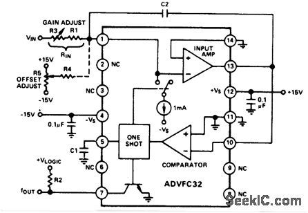
The D169 serves as a level detector and provides complementary outputs. The op amp is used to integrate the input signal VIN with a time constant of R1C1. The input (must be negative) causes a positive ramp at the output of the integrator which is summed with a nega-tive zener voltage. When the ramp is positive enough D169 outputs change state and OUT 2 flips from negative to positive. The output pulse repetition rate f0, is directly proportioned to the negative input voltage VIN. (View)
View full Circuit Diagram | Comments | Reading(0)
STROBING_LED_DISPLAY
Published:2009/7/1 21:11:00 Author:May

Applies power in sequence to segments of display, so fast that eye cannot detect flicker, to reduce drain on power supply. Input of 1000 Hz can be taken from timing chain of circuit that is driving display. 7492 divide-by-12 counter gives scan frequency of 83.3 Hz fordisplay. Binary output of 7492 is converted to 1-in-10 output by 7441 decoderfor sequential drive of 2N3904 PNP pass transistor that grounds LED which is to be lighted.-W. K.McKellips, Strobing Displays Is Cool, 73 Magazine, NovJDec. 1975, p 49-50. (View)
View full Circuit Diagram | Comments | Reading(1160)
PHASE_DETECTOR_WITH_10_BIT_ACCURACY
Published:2009/7/1 21:10:00 Author:May

Signals of identical frequency are applied to sync input (Pin 6) and to the demodulator input (Pin 4), respectively, the demodulator functions as a phase detector with output dc component being proportional to phase difference between the two inputs. The signals must be referenced to 0 V for dual supply operation or to VR/2 for single supply operation.At ± 5-V supplies, the demodulator can easily handle 7-V peak-to-peak signals. The low-pass network configured with the uncommitted amplifier dc output at Pin 1 of the device. The dc output is maximum (+ full-scale) when V1 and V2 are 180°out of phase and minimum (- full-scale) when the signals are in phase. (View)
View full Circuit Diagram | Comments | Reading(988)
FET_DIP_OSCILLATOR
Published:2009/7/1 21:10:00 Author:May

High input impedance of FET makes performance comparable to that of tube-type grid-dip oscillator. Six plug-in coils are wound on Millen 45004 1-inch 4-pin forms or equivalent. Use 150 turns No. 32 enamelfor 1.1-2.5 MHz, 77 turns No. 28 for 2.5-5 MHz, 35 turns No. 22 for 5-11 MHz, 17 turns No. 22 spaced to 1 inch for 10-25 MHz, 8.5 turns No. 22 spaced to 1 inch for 20-45 MHz and 4.5 tums No. 22 spaced to 1 inch for 40-95 MHz. Adjust R1 to set meter pointer to desired portion of scale before tuning for dip. R1 provides some control of volume when using headphones.-R.P. Turner, FET Circuits, Howard W. Sams, Indianapolis, IN, 1977, 2nd Ed., p 134-136. (View)
View full Circuit Diagram | Comments | Reading(4874)
PULSE_AND_SEQUENCE_OUTPUTS
Published:2009/7/1 21:09:00 Author:May

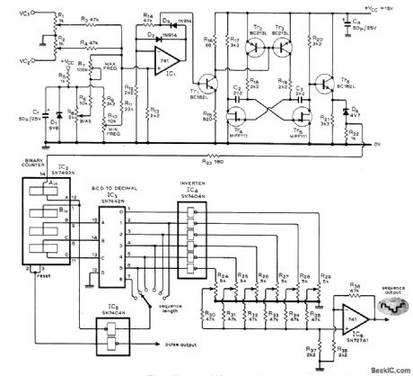
Voltagecontrolled oscillator produces sequence of steps, with amplitude of each step individually controllable up to maximum of six steps. Circuit also generates series of pulses having 1 : 1 markspace ratio. each coincident with leading edge of a step. Pair of summing inputs controls oscillator, with exponential frequency-voltage relationship extending in one range from subsonic frequencies to over 20 kHz. Used in sound synthesizer described in three-part article that gives all circuits and operating details. Applications include synthesizing sounds ranging from bird distress calls and engine noises to spoken words and wide variety of musical Instruments.-T. Orr and D W,Thomas、 Electronic Sound Synthesizer、Wireless World, Part2-Sept 1973.p 429-434 (Part 1-Aug,1973.p366-372; Part 30-ct 1973.p485-490). (View)
View full Circuit Diagram | Comments | Reading(991)
10_Hz_TO_10_kHz_VOLTAGE_FREQUENCY_CONVERTER
Published:2009/7/1 21:09:00 Author:May

View full Circuit Diagram | Comments | Reading(812)
INEXPENSIVE_RADIO_CONTROL_USES_ONLY_ONE_SCR
Published:2009/7/1 21:08:00 Author:May
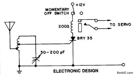
A simple and effective receiver for actuating garage doors, alarms, warning systems, etc.The SCR, which has a very low trigger current 30μA is typical-it requires an input power of only 30μW to activate the relay. A high Q tuned antenna circuit assures rejection of spurious signals. A whip or wire antenna is adequate up to 100 feet from a low power transistor transmitter. A momentary-off switch resets the circuit. (View)
View full Circuit Diagram | Comments | Reading(790)
SINGLE_LED_CAN_INDICATE_FOUR_LOGIC_STATES
Published:2009/7/1 21:07:00 Author:May
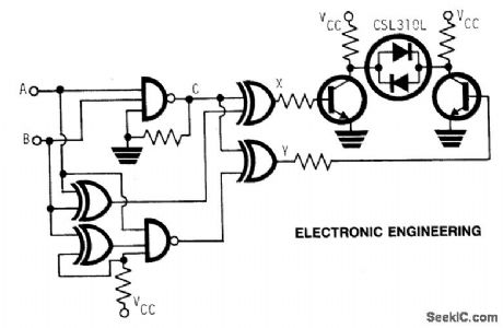
The LED is the CSL310L which contains a red LED and a green LED connected back to back and mounted close together in a single moulding. The LED can emit red or green light by controlling the polarity of the applied voltage and if the polarity is switched at a rate of several hundred Hertz the emitted light appears yellow. The four combinations of inputs A and B can therefore be converted to four LED states-red, green, yellow and off. The truth table shows the LED colors corresponding to the combinations of A and B levels.
Truth TableA B X Y LED Color1 0 0 1 0 red0 1 0 0 off1 0 0 1 green1 1 C C yellow
(View)
View full Circuit Diagram | Comments | Reading(614)
TACHOMETER,SINGLE_PULSE_GENERATOR,POWER_LOSS_DETECTOR,PEAK_DETECTOR
Published:2009/7/1 21:06:00 Author:May

A positive going input charges C through the IN4148 and R. The diode keeps the scs off.A negative going input supplies anode-gate current triggering on the scs discharging C through RL. (View)
View full Circuit Diagram | Comments | Reading(1080)
VOLTAGE_CONTROLLED_OSCILLATOR_2
Published:2009/7/1 21:04:00 Author:May

View full Circuit Diagram | Comments | Reading(722)
HIGH_FREQUENCY_PEAK_DETECTOR
Published:2009/7/1 21:04:00 Author:May

National Semiconductor's DP8464B is primarily intended for use in disk systems as a pulse detector. However it can be easily used as a general purpose peak detector for analogue signals up to 5 MHz. The chip can handle signals between 20 and 66 mV peak-to-peak. The circuit includes a filter with constant group delay characteristics to band limit the signal. Typically the -3 dB point for this filter will be at about 1.5 times the highest frequency of interest. This differentiator network between pins 1 and 24 can be as simple as a capacitor, or can be more complex to band limit the differentiator response. (View)
View full Circuit Diagram | Comments | Reading(834)
SCR_HORIZONTAL_SWEEP
Published:2009/7/24 3:48:00 Author:Jessie

Scr, fired by trigger pulse at start of retrace, transfers to yoke coil the energy stored in 1.27-mfd capacitor C. At end of retrace, energy transfer is completed, damper diode turns on, and energy in yoke returns to supply source E1,giving linear sweep current through yoke. Scr can be General Electric C35, C36, or C40 series. Yoke is 200 mkrohenrys.-T. Tarui, New Deflection Circuit Uses SCR, Saves Power, Electronics, 36:32, p 56-57. (View)
View full Circuit Diagram | Comments | Reading(559)
GAME_FEEDER_CONTROLLER
Published:2009/7/1 21:04:00 Author:May
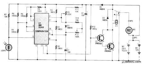
The circuit is built around an LM339 quad comparator, U1, which forms the basis of a Schmitt trigger, timer circuit, and a window comparator. One comparator within the LM339 (pins 1, 7, 6), plus LDR1, R4, R5, R6 and R8, is used as a Schmitt trigger.The timer circuit (which receives its input from the Schmitt trigger) consists of R9, R10, R11, R13. The last two-fourth's of U1 (pins 8, 9, 10, 11, 13 and 14) are wired as a window comparator. The two inputs to the window comparator are derived from the charge on capacitor C1-which is fed to pins 9 and 10 of U1. The other inputs are picked from two points along a voltage-divider network, consisting of R1, R2, and R3. Diode D1 is used as a blocking diode, forcing capacitor C1 to discharge through R10 and R13.The window comparator looks for any voltage falling between one-third and two-thirds of the supply voltage. When the voltage falls between those two points, the output of the window comparator (pins 13/14) goes high. Transistors Q1, and Q2 are turned on, when the pins 13/14 junction goes high, energizing the relay, K1. The energized relay provides a dc path to ground, activating the motor, Ml, which reloads the feeder. The timer circuit also provides immunity from triggering, due to lightning. The on-time of relay K1 is determined by the charge cycle of C1, R11, and R9 or the discharge cycle of C1, R10, and R13. Changing the value of either a resistor or the capacitor, changes the timing cycle. (View)
View full Circuit Diagram | Comments | Reading(3481)
VOLTAGE_CONTROLLED_OSCILLATOR_1
Published:2009/7/1 21:03:00 Author:May

View full Circuit Diagram | Comments | Reading(745)
OFF_LINE_24_V_100_W_DC_SUPPLY_
Published:2009/7/24 3:48:00 Author:Jessie

Today's electronic systems often rely on distributed power to support a myriad of control functions. This contrasts with historical approaches, which provided a regulated dc voltage to each of the subsystems with an off-line converter, often an expensive off-the-shelf box with less-than-optimal reliability. Shown here is a discrete approach that simplifies the task of distributed power design, saving time and money during system design. The LT1105 current-mode PWM control IC makes a simple, low-cost, yet highly reliable distributed power supply with the added advantage of a customizable footprint. The 24-V output is regulated to better than ±1 percent over a line range of 90 to 260 Vac and an 8:1 dynamic load range. A maximum output current of 4.2 A is available for a total of 100 W. All components, including the transformer, are specified in this design. The trans-former meets international safety standards UL 1950 and IEC950. This transformer and others that provide 36 or 48 V at 100 W are available off the shelf. The LT1105 uses unique design techniques, eliminating the optocoupler feedback normally found in off-line supplies, yet enabling the regulator to provide tight line and load regulation. A totem-pole output drives the gate of an external high-voltage FET (Q1), and switch current is monitored by sense resistor R22. Short-circuit protection is provided by burp mode operation, whereby the LT1105 will continuously shut down and restart during the fault condition. (View)
View full Circuit Diagram | Comments | Reading(1611)
ENLARGER_TIMER
Published:2009/7/24 3:24:00 Author:Jessie

This fairly accurate design is also suitable for color work. Unlike many simple timer designs, this unit is based around the LM3905N 8-pin D.I.L. precision timer IC, which repeats the timing period very consistently with little drift, although the accuracy of the timer depends on the tolerance of the components used. In the circuit diagram, IC1 is an LM3905N timer whose period is determined by an external RC network selected by switches S1 and S2. The formula for the time period is t=RC, where t is in seconds, R is in ohms, and C is in farads. Switch S1 is a single-pole, 12-way rotary type which selects among timing resistors R1 to R11. S2 is a three-pole, four-way rotary switch that progressively adds C1 to C3 in parallel with C4, thereby adjusting the timing capacitance range. In conjunction with the 1-percent resistor network (R1 to R11), each lμ/1M pair represents a 1-s period; hence, the maximum possible period is 44 s. Timing is initiated by closing switch S3. A floating output transistor within IC1 drives a PNP buffer, which, in turn, operates relay RLA. The circuit requires roughly a 12-V rail, and the relay coil is chosen accordingly. The IC will operate from 4.5 to 40 Vdc, and a standard full-wave power supply can be used. The relay contacts RLA1 switch on the enlarger bulb, and a separate FOCUS switch (S5) can be included across the relay contacts (or perhaps drive the relay coil manually), if desired. (View)
View full Circuit Diagram | Comments | Reading(4762)
| Pages:1169/2234 At 2011611162116311641165116611671168116911701171117211731174117511761177117811791180Under 20 |
Circuit Categories
power supply circuit
Amplifier Circuit
Basic Circuit
LED and Light Circuit
Sensor Circuit
Signal Processing
Electrical Equipment Circuit
Control Circuit
Remote Control Circuit
A/D-D/A Converter Circuit
Audio Circuit
Measuring and Test Circuit
Communication Circuit
Computer-Related Circuit
555 Circuit
Automotive Circuit
Repairing Circuit