
Circuit Diagram
Index 1160
SECONDARY_STANDARD_FOR_100_AND_10_kHz
Published:2009/7/2 0:52:00 Author:May
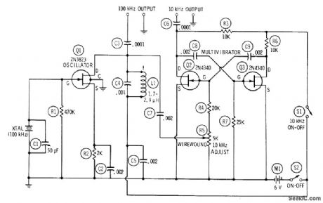
Combination of 100-kHz crystal oscillator and 10-kHz MVBR provides 100-kHz harmonics far up into high-frequency spectrum, with each 100-kHz interval subdivided by harmonics of MVBR using two FETs. Oscillator is tuned to crystal frequency whh Miller 42A223CBl or equivalent slug-tuned coil L1. C1 ad justs crystal frequency over narrow range for standardizipg against WWV transmissions. Synchronizing 100-kHz voltage is injected into MVBR through R5.-R. P. Turner, FET Circuits, Howard W. Sams, Indianapolis, IN, 1977, 2nd Ed., p 127-129. (View)
View full Circuit Diagram | Comments | Reading(904)
LOW_PASS_WITH_3_kHz_CUTOFF
Published:2009/7/2 0:51:00 Author:May
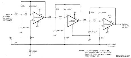
Used in computer music system to suppress high-fidelity distortion resulting from steps in sine-wave output of DAC. Article covers complete computer synthesis of music by microprocessor and gives frequency table. program for generating four simultaneous musical voices, and song table for encoding The Star Spangled Banner in four-part harmony, using 5 bytes per musical event.-H. Chamberlin,A Sampling of Techniques for Computer Performance of MusiC.BYTE.Sept.1977.p62-66.68-70.72.74.76-80.and 82-83. (View)
View full Circuit Diagram | Comments | Reading(535)
LOW_POWER_AUDIO_AMPLIFIER
Published:2009/7/2 0:46:00 Author:May
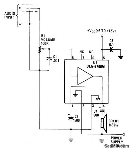
Circuit Notes
The amplifier operates from supplies ranging up to 12 volts, and operates(with reduced volume)from supply voltages as low as 1.8 volts without having distortion rise to unacceptable levels.(Its power requirements make it suitable for solar-cell application.)Components external to the integrated circuit, U1, consist of four capacitors and a potentiometer for volume control. Capacitor C3 is for decoupling, low-frequency roll-off, and power-supply ripple rejection. Capacitor C4 is an electrolytic type that couples the audio output to an 8 to 32 ohm speaker that is efficient. (View)
View full Circuit Diagram | Comments | Reading(615)
ATTACK_DECAY
Published:2009/7/2 0:46:00 Author:May
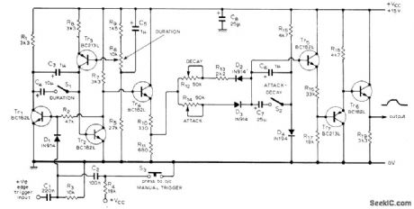
Waveform generator produces approximate rectangular waveform having exponential rise (attack) and exponential decay, initiated either by manual trigger or electronic signal derived from other circuits of sound synthesizer. All characteristics of waveform are arbitrarily variable. Three-part article describes circuit operation and gives all other circuits used in synthesizer for generating wide variety of musical and other sounds-T Orr and D W Thomas.Electronic Sound Syntheslzer.Wireless World,Part 3-Oct 1973.p485-490(Part 1-Aug .1973、 p 366-372; Part 2-Sept 1973.p 429-434) (View)
View full Circuit Diagram | Comments | Reading(1350)
VCO_SOUND_SYNTHESIZER
Published:2009/7/2 0:43:00 Author:May

Developed for use in instrument capable of duplicating variety of sounds ranging from bird distress calls and engine noises to spoken words and wide variety of musical instruments. Three-part article gives all circuits and describes their operation in detail. Heart of oscillator is triangle and square-wave generator built around IC Schmitt trigger. Ramp rate and operating frequency are varied by changing drive voltage or gain of integrator. Similar VCO in synthesizer also produces sine, pulse, and ramp waveforms.-T. Orr and D. W. Thomas, Electronic sound synthesize, Wire-less World, part 1-Aug. 1973, p 429-434; Part 3-Oct. 1973, p 485-490. (View)
View full Circuit Diagram | Comments | Reading(819)
BULL_HORN
Published:2009/7/2 0:42:00 Author:May

Circuit Notes
The input audio signal is fed to pin 3 of U1, an LM386 low-voltage amplifter, via C3 and R1. Potentiometer R1 sets the drive or volume level. U1, which serves as a driver stage, can be set for a gain of from 20 to 200. The output of U1 at pin 5 is fed to U2-a 377 dual two-watt amplifier connected in parallel to produce about four watts of output power-at pins 6 and 9 via C4 and C5. Frequency stability is determined by R2, R4, and C10 on one side, and the corresponding components R6, R5, and C9 on the other side. The outputs of the two amplifiers (at pins 2 and 13) are capacitively coupled to SPKR1 through C6 and C7. (View)
View full Circuit Diagram | Comments | Reading(2)
TROMBONE_CIRCUIT
Published:2009/7/2 0:42:00 Author:May
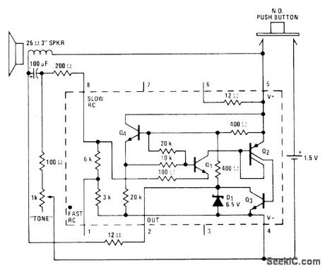
Unique arrangement for driving 25-ohm loudspeaker with National LM3909 IC operating from 1.5-V cell permits generation of slide tones resembling those of trombone. Operation is based on use of voltage generated by resonant motion of loudspeaker voice coil as major positive feedback for IC. Loudspeaker is mounted in roughly cubical box having volume of about 64 in, with one end of box arranged to slide in and out like piston. Positioning of piston and operation of pushbutton permit playing reasonable semblance of simple 15 V tune. IC, loudspeaker, and battery are mounted on piston, with 2 1/2-in length of 5/16-in tubing provided to bleed air in and out as piston is moved, without affecting resonant frequency. Frequency of oscillator becomes equal to resonant frequency of enclosure.- Linear Applications, Vol. 2, National Semiconductor, Santa Clara, CA, 1976, AN-154, p 6. (View)
View full Circuit Diagram | Comments | Reading(553)
AUDIO_FOR_COMPUTER_MUSIC
Published:2009/7/2 0:40:00 Author:May

Wideband low-power audio amplifier was developed for use with DAC and low-pass active filter to create music with microprocessor.-H Chamberlin, A Sampling of Techniques for Computer Performance of Music, BYTE, Sept 1977, p 62-66、68-70, 72, 74, 76-80, and 82-83. (View)
View full Circuit Diagram | Comments | Reading(693)
AUDIO_POWER_AMPLIFIER
Published:2009/7/2 0:40:00 Author:May
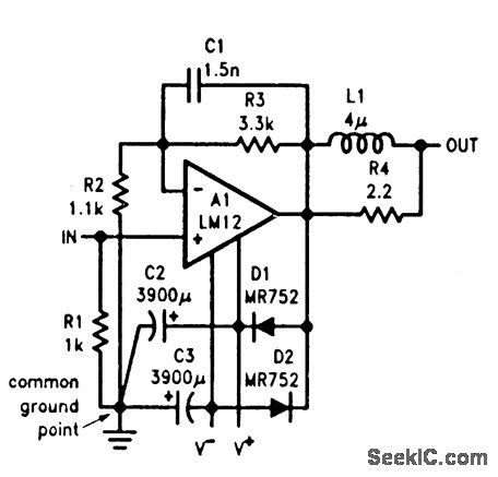
Circuit Notes
Output-clamp diodes are mandatory because loudspeakers are inductive loads. Output LR isolation is also used because audio amplifiers are usually expected to handle up to 2 μF load capacitance. Large, supply-bypass capacitors located close to the IC are used so that the rectifted load current in the supply leads does not get back into the amplifier, increasing high-frequency distortion. Single-point ground-ing for all intemal leads plus the signal source and load is recommended to avoid ground loops that can increase distortion. (View)
View full Circuit Diagram | Comments | Reading(0)
TREMOLO_CONTROL
Published:2009/7/2 0:40:00 Author:May

National LM324 opamp connected as phase-shift oscillator operates at variable rate between 5 and 10 Hz set by speed pot. Portion of oscillator output is taken from depth pot and used to modulate ON resistance of two 1N914 diodes operating as voltage-controlled attenuators. Input should be kept below 0.6 V P-P to avoid undesirable clipping. Used for producing special musical effects.- Audio Handbook, National Semiconductor, Santa Clara, GA, 1977, p 5-11-5-12. (View)
View full Circuit Diagram | Comments | Reading(703)
TUNING_FOR_EQUAL_TEMPERAMENT
Published:2009/7/2 0:39:00 Author:May
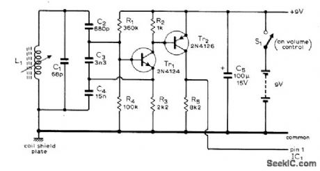
Instrument described enables anyone to tune such instruments as organ, piano, and harpsichord in equal temperament with accuracy approaching that of professional tuner. Only requirement is ability to hear beats between two tones sounded together. Master oscillator circuit shown generates 250.830 kHz for feeding to first of five ICs connected as programmable divider that provides 12 notes of an octave as 12 equal semitones differing from each other by factor of 1.0594. Article gives suitable power amplifier to fit along with divider connections and detailed instructions for construction, calibration, and use.-W. S. Pike, Digital Tuning Aid, Wireless World, July 1974, p 224-227. (View)
View full Circuit Diagram | Comments | Reading(604)
SIMULATION_OF_FLANGING
Published:2009/7/2 0:38:00 Author:May

Sound-effect circuit sometimes called phase shifter simulates playing of two tape recorders having same material while varying speed of one by pressing on flange of tape reel. Resulting time delay causes some signals to be summed out of phase and canceled. Effect is that of rotating loudspeaker or of Doppler characteristic. Uses two LM348 quad opamps, two AM9709CN quad JFET devices, and one LM741 opamp. Phase-shift stages are spaced one octave apart from 160 to 3200 Hz in center of audio spectrum, with each stage providing 90' shift at its frequency. JFETs control phase shifters. Gate voltage of JFETs is adjusted from 5 V to 8 V either manually with foot-operated rheostat or automatically by LM741 triangle-wave generator whose rate is adjustable from 0.05 Hz to 5 Hz.- Audio Hand-book, National Semiconductor, Santa Clara, CA, 1977, p 5-10-5-11. (View)
View full Circuit Diagram | Comments | Reading(1968)
2_TO_6_W_AUDIO_AMPLIFIER_WITH_PREAMPLIFIER
Published:2009/7/2 0:38:00 Author:May
Circuit NotesThe monolithic integrated audio amplifier circuit is especially designed for portable radio and recorder applications and delivers up to 4 W in a 4 ohm load impedance. (View)
View full Circuit Diagram | Comments | Reading(504)
BASIC_UJT_ORGAN
Published:2009/7/2 0:38:00 Author:May

Switches give choice of five audio frequencies for simple transistor oscillator driving loudspeaker. Adiust R1 for best combination of sounds. Capacitorvalues can be changed to give other frequencies. Ideal for classroom demonstrations.-F. M. Mims. Electronic Music Projects. Vol. Radio Shack. Fort Worth. TX. 1977. 2nd Ed., p 37-43. (View)
View full Circuit Diagram | Comments | Reading(1150)
KEYED_FREE_RUNNING_MVBR
Published:2009/7/2 0:37:00 Author:May

One section of Exar XR-2556 dual timer is operated in free-running mode, with other section used to provide ON/OFF keying. Frequency of oscillator is set by RA, RB, and C2. Timer 1 operates as mono MVBR with output connected to reset pin 8 of timer 2. Trigger drives pin 1 of timer 1 high, keying timer 2 on and producing tone-burst output for duration set by R1 and C1. Supply voltage is 4.5-16 V.- Timer Data Book, Exar Integrated Systems, Sunnyvale, CA, 1978, p 23-30. (View)
View full Circuit Diagram | Comments | Reading(837)
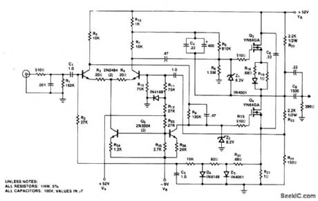
25_WATT_AMPLIFIER
Published:2009/7/2 0:36:00 Author:May

Transistors are used for current sources.Base drive for these transistors is de-rived from the main power supply VA, so that their collector current is proportional to the rail voltage. This feature holds the voltage on the diff-amp collectors close to VA/2.The sensitivity of IQ to VA is about 3.4 mA/volt when Vg is held constant; the sensitivity of IQ to VB is -15 mA/volt when VA is held constant. In a practical amplifier with a non-regulated supply, variations in power output will cause fluctuations in VA, but will not affect Vg; therefore, having IQ increase slightly with power output will tend to compensate for the 3.4 mA/volt IQVA sensitivity. In the case of line voltage variations, since VA is about five times Vg, the sensitivities tend to cancel, leaving a net sensitivity of about 2 mA/volt. (View)
View full Circuit Diagram | Comments | Reading(697)
EDGE_TRIGGERED_MONO
Published:2009/7/2 0:36:00 Author:May

Output pulse width is precisely determined by external clock frequency and countdown factor N of 74C193 binary counter (t = N/f). Pulse is generated on rising edge of input, with output remaining high until count N is reached by binary counter. Counter resets and output returns instantly to zero if input pulse goes to zero before count of N. Value of N depends on which two counter outputs are connected to two-input NAND gate. With 74C193, 11 values of N between 1 and 16 are possible; with CD4013, values of N can range from t to 24,576.-R. L. Anderson, Digital One-Shot Produces Long, Accurate Pulses, EDN Magazine, March 5, 1978, p 127. (View)
View full Circuit Diagram | Comments | Reading(729)
LM3900_AS_MONO
Published:2009/7/2 0:35:00 Author:May

R4 holds output high normally, so C1 is charged almost to V+ level through D1. Negative input trigger forces output of current-differencing amplifier low, and C1 discharges through R1. When decreasing current through R2 approaches current in R3 (when voltage across C1 is about one-third of V+), output switches to high and returns circuit to standby state. Pulse width, equal to 1.1R1C1, can be programmed easily by using pot or some form of manual or electronic switching for R1 .-W. G. Jung, IC Op-Amp Cookbook, Howard W. Sams, Indianapolis, IN, 1974, p 510-512. (View)
View full Circuit Diagram | Comments | Reading(596)
PULSE_TRIGGERED_MONO
Published:2009/7/2 0:33:00 Author:May

Combination of two ICs generates pulse having width precisely determined by external clock frequency and countdown factor N of 74C193 binary counter; time t in seconds is equal to N divided by frequency in hertz. With 74C193, 11 values of N are possible (1-6, 8-10, 12, and 16). With CD4013 14-stage counter, values of N can range from 1 to 24,576. Input pulse must be shorter than out-put pulse. Value of N depends on which two counter outputs are connected to two-input NAND gate.-R. L. Anderson, Digital One-Shot Produces Long, Accurate Pulses, EDN Magazine, March 5, 1978, p 127. (View)
View full Circuit Diagram | Comments | Reading(621)
LOGIC_CONTROL
Published:2009/7/2 0:32:00 Author:May

External circuit modification shown for 555 timer makes initial pulse more nearly equal to subsequent pulses and makes circuit deliver low output when power is applied. Optional diode ensures 50% duty cycle.-K. D. Dighe, Rearranged Components Cut 555's Initial-Pulse Errors, EDN Magazine, Jan. 5, 1978, p 82 and 84. (View)
View full Circuit Diagram | Comments | Reading(645)
| Pages:1160/2234 At 2011411142114311441145114611471148114911501151115211531154115511561157115811591160Under 20 |
Circuit Categories
power supply circuit
Amplifier Circuit
Basic Circuit
LED and Light Circuit
Sensor Circuit
Signal Processing
Electrical Equipment Circuit
Control Circuit
Remote Control Circuit
A/D-D/A Converter Circuit
Audio Circuit
Measuring and Test Circuit
Communication Circuit
Computer-Related Circuit
555 Circuit
Automotive Circuit
Repairing Circuit