
Circuit Diagram
Index 1159
Battery_operated_thermocouple_with_cold_junction_compensation
Published:2009/7/24 2:53:00 Author:Jessie

Pig. 13-32 This cold-junction thermocouple signal conditioner does not require any trim, and provides an accuracy of ±0.75℃ over the indicated range (0 to 60℃). Current consumption is about 125μA. Using the specified battery life will approach 10 y ears. Linear Technology Linear Applications Handbook, 1990 p AN23-2. (View)
View full Circuit Diagram | Comments | Reading(828)
Thermocouple_signal_conditioner_with_cold_junction_compensation
Published:2009/7/24 2:51:00 Author:Jessie
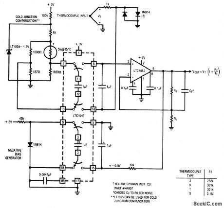
Fig. 13-31 This circuit shows a 5-V powered thermocouple signal conditioner. Cold-junction compensation is included, and the circuit allows one leg of the thermocouple to be grounded (for noise considerations). The table gives proper values for R1 for various standard thermocouples. Output scaling can be set by RF/R1 to whatever slope is desirable. Cold-junction compensation holds within ±1℃ over 0o to 60℃. Linear Technology, Linear Applications Handbook 1990, p AN 11-5. (View)
View full Circuit Diagram | Comments | Reading(987)
90_W_AUDIO_POWER_AMPLIFIER_WITH_SAFE_AREA_PROTECTION
Published:2009/7/2 1:20:00 Author:May

View full Circuit Diagram | Comments | Reading(798)
250_MHz_broadband_amplifier_15_V_supply
Published:2009/7/24 2:51:00 Author:Jessie
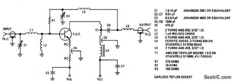
The electrical characteristics for the 2N5943 shown in this circuit are given in Fig. 2-31B. (View)
View full Circuit Diagram | Comments | Reading(666)
Freezer_alarm
Published:2009/7/24 2:50:00 Author:Jessie

Fig. 13-30 This circuit shows a very simple configuration for a freezer alarm. Such circuits are used in industrial and home freezers as well as in refrigerated trucks and rail cars. The LTC1042 is a sampled-operation window comparator. The 10 MΩ/0.05μF combination sets a sample rate of 1 Hz, and the bridge values program the internal window comparator for the outputs shown. For normal freezer operation, pin 1 is high and pin 6 is low. Over-temperature reverses this state and can trigger an alarm. Circuit current consumption is about 80μA. Linear Technology, Linear Applications Handbook 1990, p. AN23-7.
(View)
View full Circuit Diagram | Comments | Reading(1706)
Battery_powered_wall_thermostat
Published:2009/7/24 2:49:00 Author:Jessie

Fig. 13-29 This circuit shows a battery-powered thermostat using an LTC1041.Temperature is sensed using a thermistor connected in a bridge with a potentiometer to set the desired temperature. However, the bridge is not driven from the battery but from pin 7 on the LTC1041. Pin 7 is the pulsed power (Vpp) output and turns on only while the LTC is sampling the inputs, thus keeping average power drain extremely low. A lithium battery will run the circuit for at least 10 years. A 2N6660 power MOSFET in a diode bridge switches the conventional 26 Vac heater-control circuitry. The 2N6660 requires no current from the battery. Linear Technology Linear Applications Handbook 1990 p AN23-6.
(View)
View full Circuit Diagram | Comments | Reading(2122)
AUDIBLE_VISIBLE_METRONOME
Published:2009/7/2 1:19:00 Author:May
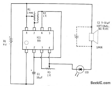
Produces uniformly spaced beats in synchronism with flashes of LED, at rate that can be adiusted with R1 from one beat every few seconds to ten or more beats per second. Use red Radio Shack 276-041 or similar LED. Add switch in series with battery to avoid disturbing setting of R1. R3 serves as volume control. Add 5-10 μF capacitor across loudspeaker to mellow beat sound if desired.-F. M. Mims. Electronic.'' Music Projects. Vol. 1. Radio Shack, Fort Worth, TX, 1977, 2nd Ed.p 55-59. (View)
View full Circuit Diagram | Comments | Reading(624)
REAR_SPEAκER_AMBIENCE(4_CHANNEL)AMPLIFIER
Published:2009/7/2 1:13:00 Author:May

Circuit Notes
Rear channel ambience can be added to an existing stereo system to extract a difference signal(R-L or L-R)which, when combined with some direct signal(R or L), adds fullness, or concert hall realism to the reproduction of recorded music. Very little power is required at the rear channels, hence an LM1877 suffices for most ambience applications. The inputs are merely connected to the existing speaker output terminals of a stereo set, and two more speakers are connected to the ambience circuit outputs. The rear speakers should be connected in the opposite phase to those of the front speakers, as indicated by the +/- signs. (View)
View full Circuit Diagram | Comments | Reading(891)
PREAMP_FOR_ACOUSTIC_PiCkUP
Published:2009/7/2 1:12:00 Author:May

National LM387 dual opamp provides switchable gain choice of ±10 dB along with bass/treble tone control and volume control. Used with flat-response piezoceramic contact pickup for acoustic stringed musical instruments such as guitar.violin. and dulcimer. Half of IC is used as controllable gain stage, and other half is used as active two-band tone-control block.- Audio Handbook. National Semiconductor. Santa Clara. CA. 1977. p 5-12. (View)
View full Circuit Diagram | Comments | Reading(3285)
WALKMAN_AMPLIFIER
Published:2009/7/2 1:08:00 Author:May
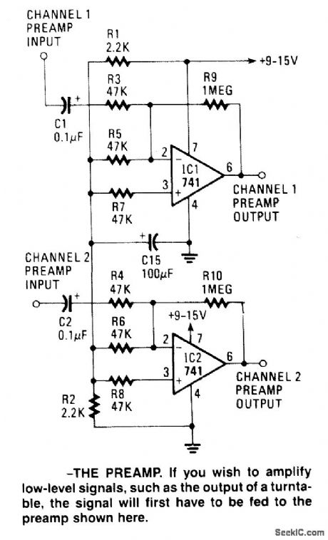
Circuit Notes
The gain of the low-cost IC is internally fixed so that it is not less than 34 dB(50 times). A unique input stage allows input signals to be referenced to ground. The output is automatically self centering to one half the supply voltage. The output is also short-circuit proof with internal thermal limiting. With a maximum supply of 15 volts and an 8 ohm load, the output is around 1.5 watts per channel. The input stage is usable with signals from 50 mV to 500 mV rms. If the amplifier is to be used with a source other than a personal stereo, such as a phonograph or an electric guitar, some type of preamplifier is required. A suitable circuit is shown. In that circuit, two 741 op amps have been configured as input amplifiers. Their input stages referenced to a common point-half the supply voltage. That voltage is derived from a voltage divider made up of RI and R2, two 2.2 k resistors. The gain of each of the 741's has been fixed at 21 by the input resistors(R9, R10). Input capacitors, C1 and C2, are used to filter out any dc component from the input signal. (View)
View full Circuit Diagram | Comments | Reading(2345)
50_MHz_CRYSTAL
Published:2009/7/2 1:07:00 Author:May

Uses microtransistor as oscillator handling 100-mW input power and giving 40-50% efficiency. Article covers construction with microcomponents and gives other microtransistor circuits for low-power amateur radio use and possible bugging applications.-B. Hoisington, Introduction to Microtransistors, 73 Magazine, Oct. 1974, p 24-30. (View)
View full Circuit Diagram | Comments | Reading(725)
UP_TO_1OO_kHz_WITH_322_TIMER
Published:2009/7/2 1:07:00 Author:May

Efficient LC oscillator uses IC timer as inverting comparator, with pinetwork LC tank as resonant circuit. Output square wave is regulated to 3 V in amplitude, independently of supply voltage; upper supply limit should be 40 V instead of value shown. Sine-wave output of oscillator may also be used extemally by adding single-supply opamp as buffer. Values shown give 10 kHz, but upper limit is 100 kHz.-W. G. Jung, Take a Fresh Look at New IC Timer Applications, EDN Magazine, March 20, 1977, p 127-135. (View)
View full Circuit Diagram | Comments | Reading(1715)
FOUR_OCTAVE_ORGAN
Published:2009/7/2 1:06:00 Author:May
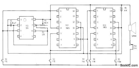
Two 7473 dual flipflops provide four frequency dividers for 555 timer connected as master tone generator. S1 gives fundamental frequency. and each succeedlig switch gives tones precisely one octave lower. Four organ applications, pushbutton switches are added to timer circuit for switching frequency-controlling capacitors or resistors to give desired variety of notes.-F. M. Mims.″Electronic Music Proiects.vol 1.″Radio Shack.Fod Wodh.TX.1977.2nd Ed.p45-53. (View)
View full Circuit Diagram | Comments | Reading(2058)
100_kHz_SINE
Published:2009/7/2 1:06:00 Author:May

Tunnel-diode sine-wave oscillator uses single GE 2J-69. Frequency is stable provided there are no drastic temperature changes, but for long-term accuracy and stability a crystal oscillator is recommended.-Circuits, 73 Magazine, May 1977, p 31. (View)
View full Circuit Diagram | Comments | Reading(970)
279611_kHz_CRYSTAL
Published:2009/7/2 1:05:00 Author:May

DT-cut quartz crystal operating in CMOS inverter pair circuit serves as efficienttiming circuit. Supply voltage can be from 5 to 15 V. With TA5987 Low-voltage equivalent of 4007, supply can be 2.5 to 5 V. Stability is 4.3 PPM, not including temperature variations.-B. Furlow, CMOS Gates in Linear Applications: The Results Are Surprisingly Good, EDN Magazine, March 5, 1973, p 42-48. (View)
View full Circuit Diagram | Comments | Reading(687)
RC_CONTROL
Published:2009/7/2 1:04:00 Author:May

Chief advantage is absence of attenuation at zero phase shift in passive RC network used to define frequency of oscillation. Output is 20 V P-P. Pilot lamp stabilizes loop gain to unity, eliminating need forthermistor.-W. R. Jackson, Oscillator Uses Passive Voltage-Gain Network, Wireless Workl, April 1975, p 175. (View)
View full Circuit Diagram | Comments | Reading(605)
5_MHz_LOW_NOISE_CRYSTAL
Published:2009/7/2 1:03:00 Author:May

Extremely low-noise series-mode crystal oscillatoris designedfor use in high-quality communication receivers. Eitherfundamental or overtone crystals can be used.-U. L. Rohde, Effects of Noise in Receiving Systems, Ham Radio, Nov. 1977, p 34-41. (View)
View full Circuit Diagram | Comments | Reading(790)
AUDIO_BOOSTER
Published:2009/7/2 1:02:00 Author:May
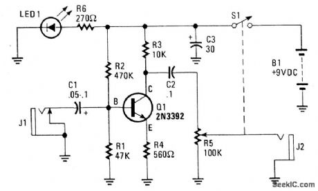
Circuit Notes
The amplifier's gain is nominally 20 dB. Its frequency response is determined primarily by the value of just a few components-primarily C1 and R1. The values of the schematic diagram provide a fesponse of ±3.0 dB from about 120 Hz to better than 20,000 Hz.Actually, the frequency response is ruler flat from about 170 Hz to well over 20,000 Hz; it's the low end that deviates from a flat frequency response. The low end's roll-off is primarily a function of capacitor C1(since RI's resistive value is fixed). If C1's value is changed to 0.1 pF, the low end's comer frequency-the frequency at which the low-end roll-off starts-is reduced to about 70 Hz. If you need an even deeper low-end roll-off, change C1 to a 1.0 pF capacitor; if it's an electrolytic type, make certain that it's installed into the circuit with the correct polarity, with the positive terminal connected to Q1's base terminal. (View)
View full Circuit Diagram | Comments | Reading(0)
ATTACK_DECAY_GENERATOR
Published:2009/7/2 0:58:00 Author:May
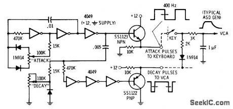
Designed for polytonic electronic music system handling more than one note at a time. Each note to be controlled is sent through voltage-controlled amplifier (VCA) whose gain is set by charge on capacitor. Attack is changed by varying charging rate. Discharge rate sets decay of individual note. To avoid having separate adjustment pot for each VCA, duty-cycle modulation is used to change charging current through resistors. Attack pulses are generated by upper three inverters forming variable-symmetry astable MVBR. Decay pulses are generated by lower three inverters connected as half-mono MVBR.
Additional half-monos can be added as needed for percussion, snubbing, and other two-step decay effects.-D. Lancaster, CM0S Cook-book.''Howard W.Sams.Indianapolis.IN.1977.p231-232 (View)
View full Circuit Diagram | Comments | Reading(677)
450_500_kHz_WOBBULATOR
Published:2009/7/2 0:54:00 Author:May
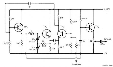
Center frequency of sweep is adjusted with C1 and C2. With appropriate coil, operation can be extended up to 10.7 MHz. Transistors can be BC107, BF115, BF194, or other equivalent. Choose value of Rx to give best waveform with transistor types used. Feedback for VCO is taken via Tr3 without phase change. If control voltage for base of Tr3 is derived from ramp out-put of oscilloscope time base, wobbulator out-put will follow variations in sweep voltage of time base.-E. C. Lay, Wobbulator, Wireless World, May 1975, p 226. (View)
View full Circuit Diagram | Comments | Reading(2882)
| Pages:1159/2234 At 2011411142114311441145114611471148114911501151115211531154115511561157115811591160Under 20 |
Circuit Categories
power supply circuit
Amplifier Circuit
Basic Circuit
LED and Light Circuit
Sensor Circuit
Signal Processing
Electrical Equipment Circuit
Control Circuit
Remote Control Circuit
A/D-D/A Converter Circuit
Audio Circuit
Measuring and Test Circuit
Communication Circuit
Computer-Related Circuit
555 Circuit
Automotive Circuit
Repairing Circuit