
Circuit Diagram
Index 1149
STEREO_PREAMPLIFIER
Published:2009/7/2 4:33:00 Author:May
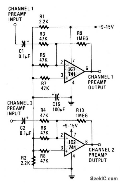
The circuit provides better than 20-dB gain in each channel. A better op-amp type will give a better noise figure and bandpass. In this circuit the roll-off is acute at 20,000 Hertz. (View)
View full Circuit Diagram | Comments | Reading(0)
TWO_GATE_SCHMlTT
Published:2009/7/2 4:33:00 Author:May
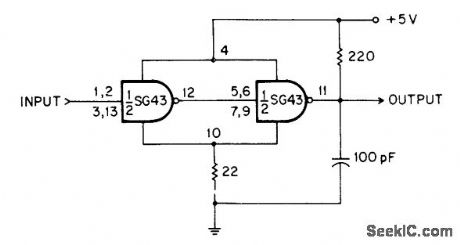
TTL inverter gates are connected in series, with small feedback resistorin common ground lead, so gates are always in opposing logic states. Resulting constqnt voltage drop across 22-ohm resistor produces constant offset voltage that is corrected by 220-ohm resistor at output terminal. With values shown, positive-going threshold is 2.4 V and negative-going threshold is 2 V.-C. J. Ulrick, Schmitt Tdgger Uses Two Logic Gates, EEE Magazine, Dee. 1970, p 54. (View)
View full Circuit Diagram | Comments | Reading(569)
NOISE_GATE_FOR_AF_PREAMP
Published:2009/7/2 4:31:00 Author:May
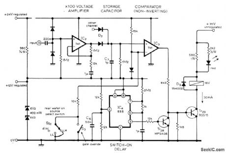
Used in highperformance phono preamplifier to mute output when there is no signal at phono input.Opamps each provide gains of about 100,Circuit controls muting reed relay serving both stereo channels of preamp. Delay switch-on using 555lC overrides noise-gate opamps. Unmarked diodes are 1 N914 or equivalent, and red LED is TIL209 or equivalent. Article covers circuit operation in detail and gives all other circuits of preamp.- D. Self. Advanced Preampli-fier Design, Wireless World, Nov 1976. p41-46. (View)
View full Circuit Diagram | Comments | Reading(831)
TRANSISTOR_HEADPHONE_AMPLIFIER
Published:2009/7/2 4:31:00 Author:May

View full Circuit Diagram | Comments | Reading(864)
AUTO_FADE
Published:2009/7/2 4:30:00 Author:May

The automatic fader drops the level of the background music when the narration comes up. The control input goes through R10, a preset audio level control, to the input of an emitter-follower buffer stage (Q1). The buffer offers a high input impedance and makes sure that the source impedance is low enough to drive the rectifier and smoothing circuit, which consist of D1, D2, and C5. The smoothed output drives a simple LED circuit. R8 and LDR1 form an input attenuator across which the output is fed via C6 and C7 to the output jack. The output at the emitter of Q1 couples to this socket through C4 and R5. R5 and R7 are a passive mixer. With 200 mV or less at the input, there isn't sufficient voltage across C5 to make Q2 turn on. Over 200 mV, Q2 does turn on to a limit, and the LED gets power. That makes the LDR's resistance fall, and signal loss through the attenuator increases. Increase the input to 350 mV rms, and you get a signal reduction of better than 20 dB. (View)
View full Circuit Diagram | Comments | Reading(1027)
TIME_DELAY_SWITCH
Published:2009/7/2 4:30:00 Author:May

Oscillator connection shown for 555 timer provides delay for switching action controlled by logic input. When logic input is 0 V, timer output is low. When logic input goes high, output remains low for delayof 0.693RBC s and then switches high. Output remains high as long as input is high.-K. D.Dighe, Rearranged Components Cut 555's lnitial-Pulse Errors, EDNMagazine, Jan. 5, 1978, p 82 and 84. (View)
View full Circuit Diagram | Comments | Reading(895)
POWER_UP_POWER_DOWN_RESET
Published:2009/7/2 4:26:00 Author:May

Output of circuit goes high at end of time interval RTUCTU, required for charging of CTU by applied 5-VDC inputsignal. When 5-V power fails, Q1, drives Q2, and Q3, off, making output low for time interval determined by RTDCTD. When CTD is discharged, output goes high again. Interruption of power thus produces negative-going pulse having variable width determined by values chosen for resistors and capacitors.-S. Rummel, Reset Circuit Detects Power Drop-Out, EDN Magazine, May 20, 1976, p 94. (View)
View full Circuit Diagram | Comments | Reading(905)
FOUR_CHANNEL_FOUR_TRACK_MIXER
Published:2009/7/2 4:25:00 Author:May
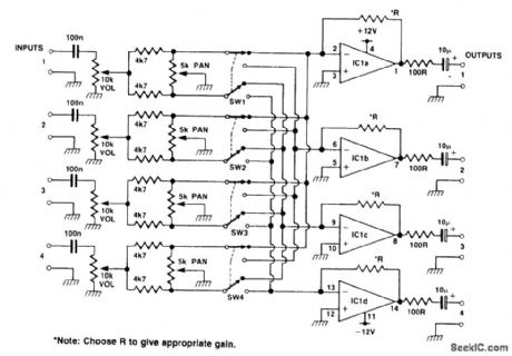
This circuit can be used as a stereo mixer as well as a four track. The quad op-amp IC gives a bit of gain for each track. The pan control allows panning between tracks one and two with the switch in the up position, and with the switch in the down position, it makes possible panning between tracks three and four. Extra channels can be added.A suitable op amp for IC1 is TL074 or similar. (View)
View full Circuit Diagram | Comments | Reading(1919)
15-3500_Hz_BANDPASS
Published:2009/7/2 4:25:00 Author:May
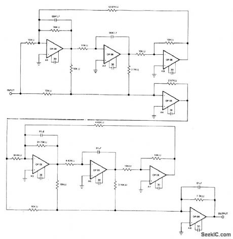
Five-pole telecommunication filter using eight Precision Monolithics op-08 opamps provides better than 30-dB attenuation in stop band.Total supply drain is only 4.8 mA for±15 V supply.- Precision Low Input Current Op Amp, Preoision Monolithics, Santa Clara, CA,1978,OP-08,p 6. (View)
View full Circuit Diagram | Comments | Reading(604)
AUDIO_DISTRIBUTION_AMPLIFIER
Published:2009/7/2 4:24:00 Author:May

The three channel output distribution amplifier uses a single TL084. The first stage is capacitively coupled with a 1.0 μF electrolytic capacitor. The inputs are at 1/2 VCC rail or 4.5 V. This makes it possible to use a single 9 V supply. A voltage gain of 10 (1 M ohm/100 k ohm) is obtained in the first stage, and the other three stages are connected as unity-gain voltage followers. Each output stage independently drives an amplifier through the 50 μF output capacitor to the 5.1 k ohm load resistor. The response is flat from 10 Hz to 30 kHz. (View)
View full Circuit Diagram | Comments | Reading(0)
LOW_DISTORTION_INPUT_SELECTOR_FOR_AUDIO_USE
Published:2009/7/2 4:23:00 Author:May
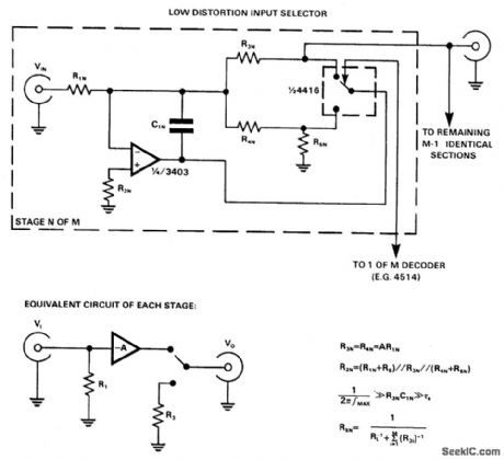
CMOS switches are used directly to select inputs in audio circuits, this can introduce unacceptable levels of distortion, but if the switch is included in the feedback network of an op amp, the distortion due to the switch can be almost eliminated. The circuit uses a 4416 CMOS switch, arranged as two independent SPDT switches. If switching transients are unimportant, R5 and C1 can be omitted, and R4 can be shorted out. However, a feedback path must be maintained, even when a channel is switched out, in order to keep the inverting input of the op amp at ground potential, and prevent excessive crosstalk between channels. (View)
View full Circuit Diagram | Comments | Reading(1006)
10_kHz_VARIABLE_Q
Published:2009/7/2 4:22:00 Author:May
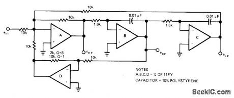
Second-order state-variable filter having center frequency of 10 kHz uses all four sections of opamp Center frequency can be tuned by varying 1.6K feedback resistors or by changing 0.01-μF feedback capacitors. Value of feedback resistor for opamp D determines Q of filter, for adjusting circuit bandwidth or damping. For higher-frequency operation, use high-speed opamps such as OP-15 or OP-16.-D. Van Dalsen, Need an Active Filter? Try These Design Aids, EDN Magazine, Nov.5,1978, p 105-110. (View)
View full Circuit Diagram | Comments | Reading(725)
NOISE_CONTROL
Published:2009/7/2 4:21:00 Author:May

Circuit is plugged into headphone jack of amateur receiver. Four-position rotary switch selects desired combination of noise-limitingdiodes for handling progressively more severe noise pulses. Adjustable AF T-notch filter limits passband over sufficient range for both phone and CW. Inductor is common 88-mH toroid. Audio peaker circuit overcomes insertion losses of filters.-S. T. Rappold. Noise Rejector. 73 Magazine. Sept. 1977. p 116. (View)
View full Circuit Diagram | Comments | Reading(629)
POLARITY_REVERSER
Published:2009/7/2 4:21:00 Author:May

Logic input controls operation of DG303 low-power analog switch providing polarity reversal for output of opamp.Low input logic gives noninverting operation because input signal then goes to pin 12 of opamp.- Analog Switches and Their Applica-tions, Siliconix, Santa Clara, CA, 1976, p 7-91. (View)
View full Circuit Diagram | Comments | Reading(1438)
MICROPHONE_MIXER
Published:2009/7/2 4:20:00 Author:May
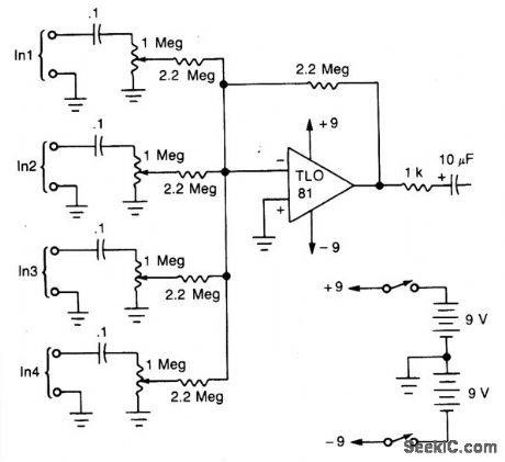
A TL081 op amp is used as a high-to-low impedance converter and signal mixer. The input impedance is approximately 1 megohm and the output impedance is about 1 kilohm. Two 9-volt batteries are used as the power source. Battery life should be several hundred hours with alkaline batteries. (View)
View full Circuit Diagram | Comments | Reading(217)
SOUND_MIXER_AMPLIFIER
Published:2009/7/2 4:19:00 Author:May

Both input signals can be independently controlled by VR1 and VR2. The balance control VR3 is used to fade out one signal while simultaneously fading in the other. The transistor provides gain and the combined output signal level is controlled by VR4 (optional). (View)
View full Circuit Diagram | Comments | Reading(616)
TRACKING_LINE_FREQUENCY_FILTER
Published:2009/7/2 4:14:00 Author:May

Improvements in commutating RC network filter extend dynamic range without sacrificing signal bandwidth, for reducing interference at fundamental of power-line frequency and harmonics up to fifth. Although values in circuit are for British 50-Hz mains frequency, circuit can readily be adapteU for 60-Hz rejection. Operation involves commutating 16 capacitors electroni.cally at 16 times line frequency, Article gives one method of doing this, by driving two 8-way multiplexors alternately. Each multiplexec has eight MOSFETg, each switched on in turn by consecutive input clock pulses. Circuit details, design equations, and performance graphs are given Three-position swith gives choice of filer characteristics.-K. F. Knott and L. Unsworth, Mains Rejection Tracking Filter, Wireless World,Oct.1974, p 375-379. (View)
View full Circuit Diagram | Comments | Reading(862)
PULSE_RECEIVER_TESTER
Published:2009/7/24 2:26:00 Author:Jessie

Simulates fold conditions encountered by pulse receivers use in ionospheric soundings, by supplying powerful pulse followed by weak pulse, with variable time separation. Weak pulse can be moved through fixed strong pulse without addition of pulse amplitudes. Uses cathode-follower mixer pulser and c-w oscillator pulsing a buffer.-K. Perry, Transmitter Simulator Tests Pulse and Phase-Palh Receivers, Electronics, 33:41, p 67. (View)
View full Circuit Diagram | Comments | Reading(560)
CURRENT_SLOPE_CONTROL_FOR_RESISTANCE_WELDING
Published:2009/7/24 2:25:00 Author:Jessie

Varies buildup and decay rates of, current, to increase weld quality and uniformity. Consists essentially of variable resistance inserted in phase-shift circuit of main welding control.-J. Markus and V. Zeluff, Handbook of Industrial Electronic Control Circuits, McGraw-Hill, New York, 1956, p 340. (View)
View full Circuit Diagram | Comments | Reading(1189)
Differential_sensing_for_type_J_grounded_thermocouple
Published:2009/7/24 2:25:00 Author:Jessie

Fig. 13-17 This circuit also provides full-differential sensing as in Fig, 13-16, but for type-J grounded thermocouples.Note that the sensor output is subtracted from the LT1025. Linear Technology Linea Applications Handbook 1990 p AN28-7. (View)
View full Circuit Diagram | Comments | Reading(805)
| Pages:1149/2234 At 2011411142114311441145114611471148114911501151115211531154115511561157115811591160Under 20 |
Circuit Categories
power supply circuit
Amplifier Circuit
Basic Circuit
LED and Light Circuit
Sensor Circuit
Signal Processing
Electrical Equipment Circuit
Control Circuit
Remote Control Circuit
A/D-D/A Converter Circuit
Audio Circuit
Measuring and Test Circuit
Communication Circuit
Computer-Related Circuit
555 Circuit
Automotive Circuit
Repairing Circuit