
Circuit Diagram
Index 1153
1_GHz_MANCHESTER_DECODER
Published:2009/7/2 3:31:00 Author:May

Use of ECL flip-flop with toggle rates above 1 GHz makes , decoding of bit rates approaching gigabit speeds feasible. Article gives step-by-step destgn procedure for 48-Mb telemetry application using PCM over single optical-fiber cable.-B.R.Jarrett,Could You Design a High-Speed Manchester-Code Demodulator?, EDN Magazine, Aug. 20, 1974, p 75-80. (View)
View full Circuit Diagram | Comments | Reading(1891)
SEWING_MACHINE_SUPPRESSION
Published:2009/7/2 3:30:00 Author:May
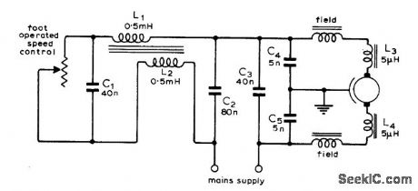
Circuit is used to suppress clicks from speed control aswell as intelf erence produced by motor itselfinsound and television broadcast bands.-A s McLachlan J .H .Ainley and R.J Harry. Radio Interfererce-a Review Wireless World. June1974.p 191-195. (View)
View full Circuit Diagram | Comments | Reading(493)
BASIC_SINGLE_SUPPLY_VOLTAGE_REGULATOR
Published:2009/7/2 3:26:00 Author:May

Circuit NotesThe circuit uses a CA3140 BiMOS op amp capable of supplying a regulated output that can be adjusted from essentially 0 to 24 volts. (View)
View full Circuit Diagram | Comments | Reading(667)
ALARM_DRIVES_PAGING_BEEPER
Published:2009/7/2 3:24:00 Author:May
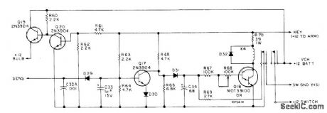
Complete protection of vehicle is provided by multiplicity of door-switch, mat-switch, vibration, motion, and other sensors connected to common sen-sor input of alarm switching circuitthat controls radio pager, 1-W GE Voice Command II trans-mitter operating around 147 MHz, 100-W electronic siren, and power horns. Closing of con tacts in any sensor grounds common input (assuming keylock switch has been closed to arm circuit by applying +12 V), applying power to siren and pager system. Range is about 1 mi for Motorola Pageboy II cigarette-pack-size pager receiver. Article describes construction, operation, and installation in detail and gives complete circuit of pager.-J. Crawford, Build a Beeper Alarm, 73 Magazine, Oct. 1977, p 68-77.
(View)
View full Circuit Diagram | Comments | Reading(841)
ARIABLE_CURRENT_SOURCE,100_mA_TO_2_AMP
Published:2009/7/2 3:24:00 Author:May
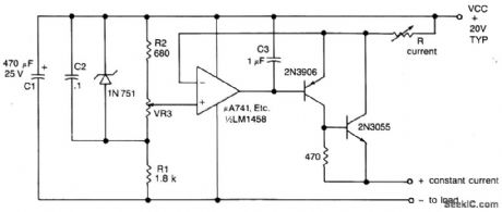
Circuit NotesThe output current is set by the resistor R in the collector of Tr2, which may be varied to offer a range of output currents from 100 mA to 2 A with fine control by means of VR3 which varies the reference voltage to the non-inverting input of the op amp. The feedback path from the output to the inverting input of the op amp maintains a constant voltage across R, equal to(VCC-VIN)/and hence a constant current to the load given by(VCC-VIN)/R. (View)
View full Circuit Diagram | Comments | Reading(589)
MULTIPLE_FEEDBACK_BANDPASS_FILTER
Published:2009/7/2 3:22:00 Author:May


The op amp is connected in the inverting mode. Resistor R3 from the output to the inverting input sets the gain and current through the frequency-determining capacitor, C1. Capacitor C2 provides feedback from the output to the junction of R1 and R2.C1 and C2 are always equal in value. Resistor R2 may be made adjustable in order to adjust the center frequency which is determined from:When designing a filter of this type it is best to select a value for C1 and C2, keeping them equal. Typical audio filters have capacitor values from 0.01,μF to 0.1,μF which will result in reasonable values for the resistors. (View)
View full Circuit Diagram | Comments | Reading(0)
INPUT_NOISE_TEST_CIRCUIT
Published:2009/7/2 3:20:00 Author:May

Used for mealsuring noise immunity of emitter-coupled logic to transient signal on input line. Supply voltages used permit terminating logic outputs to ground through 50-ohm CRO probe. Accurate bias provided by power supply is used to set input logic levels. 450-ohm resistor is used in series with 50-ohm input of CRO to isolate input; this gives 10:1 amplitude attenuation while still providing accurate picture of input noise.-B. Blood. AC Noise Immunity of MECL 10.000 lntegrated Circuits. Motorola, Phoenix. AZ. 1972, AN-592. (View)
View full Circuit Diagram | Comments | Reading(677)
SOUND_ACTIVATED_SWITCH
Published:2009/7/2 3:20:00 Author:May

Can be used as sensor for burglar alarm or for turning on su'-veillance tape recorder to monitor conversa-tions. R8, is adjusted to give desired sensitivity at which A2, triggers switch Q1, to provide 200-mA load current and turn on indicator LED. First section of LM339 quad comparator serves as amplifier and detector providing gain of 100. Second comparator compares DC output of first with reference level selected by R8.-D. ft. Mor-gan, Sound Turns Switch On, EDN Magazine, Aug. 5, 1978, p 82 and 84. (View)
View full Circuit Diagram | Comments | Reading(3050)
BANDPASS_AND_NOTCH_FILTER
Published:2009/7/2 3:19:00 Author:May

The Quad op amp MC4301 is used to configure a ftlter that will notch out a given frequency and produce that notched-out frequency at the BP terminal, useful in communications or measurement setups. By proper component selection any frequency ftlter up to a few tens of kilohertz can be obtained. (View)
View full Circuit Diagram | Comments | Reading(793)
WIRE_CUTTING_ALARM
Published:2009/7/2 3:17:00 Author:May

SCR normally acts as open circuit in series with 12-VDC alarm relay because grid is made negative by voltage divider consisting of 100K in series with500 ohms. If ground on 500-ohm resistor is re-moved, as by removal of tape player or CB set from car by thief, gate becomes more posltive and SCR conducts, to energize relay, sound hom, and make headlights shine brightly. Ad-ditional triggering SCRs or alarm switches can be added as shown outside of dashed area for basic alarm.-A. Szablak, Another Burglar Alarm, 73 Magazine, May 1974, p 45-46. (View)
View full Circuit Diagram | Comments | Reading(728)
7_SEGMENT_TO_BCD
Published:2009/7/2 3:17:00 Author:May
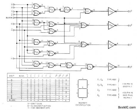
Uses six CMOS packages to convert 7-segment display to corresponding four-line positive-logic BCD code for digits 0-9. Added feature is blank input which, when high,foroes blank code(1110 or 1111)into readout,for use in suppressing leading zeros with some types of data storage.Use 4010 in place of 4009 for Z6 when negative-logic BCD output is required.—R. Sturla, Real-Time 7-Seg-ment to BCD Converter, EDN Magazine, June 20, 1973, p 89. (View)
View full Circuit Diagram | Comments | Reading(7823)
MICROPOWER_BANDGAP_REFERENCE_SUPPLY
Published:2009/7/2 3:16:00 Author:May

Circuit NotesThe circuit uses a CA3440 BiMOS op amp and CA3086 transistor array. The no-load current from 5-volt supply is 1.5 μA. Load current can go as high as 200 pA and still maintain output voltage regulation within 0.05%. (View)
View full Circuit Diagram | Comments | Reading(598)
Battery_status_indicator
Published:2009/7/24 2:32:00 Author:Jessie

This circuit is designed for a 9-V battery. D1 begins dimming noticeably below 7 V and extinguishes at 6 V. If the dimming function is not required, remove R3 and make R1 340 kΩ. D1 will then remain at normal brilliance until the battery goes below 6 V. (View)
View full Circuit Diagram | Comments | Reading(0)
216_MHz_high_gain_amplifier_15-V_supply
Published:2009/7/24 2:32:00 Author:Jessie
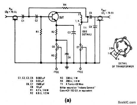
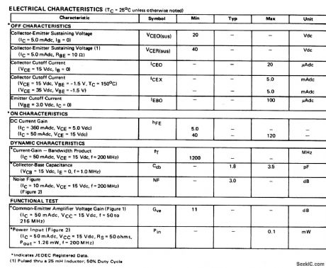
The electrical characteristics for the 2N5019 shown in this circuit are given in Fig.2-22B. (View)
View full Circuit Diagram | Comments | Reading(495)
ACTIVE_BANDPASS_FILTER
Published:2009/7/2 3:16:00 Author:May


The circuit is a two-pole active filter using a TL081 op amp. This type of circuit is usable only for Qs less than 10. The component values for this filter are calculated front the following equations.The values shown are for a center frequencyof 800 Hz. (View)
View full Circuit Diagram | Comments | Reading(1456)
SQUIB_SIMULATOR
Published:2009/7/24 2:32:00 Author:Jessie

Simulates electrical characteristics of primer or squib of propellant-actuated fastener used in missiles and space systems for vehicle separation. Has very low impedance prior to firing, and infinite impedance after firing. Useful for testing firing circuits in laboratory where firing of actual squib would create disturbing sound.-C. S. Lewis, Electronic Squib Simulator, EEE, 10:9, p 24-25. (View)
View full Circuit Diagram | Comments | Reading(1287)
TIME_TO_VOLTAGE
Published:2009/7/2 3:15:00 Author:May

Time period of negative gating signal determines amplitude of linear output ramp generated by integrator opamp. Amplitude of ramp, proportional to input time, is observed on calibrated screen of oscilloscope.—G. B. Clayton, Experiments with Operational Amplifiers, Wireless World, Sept.1973, p 447-148 (View)
View full Circuit Diagram | Comments | Reading(716)
Linearized_platinum_RTD_signal_conditioner
Published:2009/7/24 2:32:00 Author:Jessie

Fig. 13-19 This circuit provides complete linearized signal conditioning for a platinum RTD (Rosemount 118MFRTD). To calibrate, substitute a precision decade box (General Radio 1432k) for Rp Set the box to the 0℃ value (100.00Ω) and adjust the offset trim (50 kΩ zero adjust) for a 0.00-V output. Next, set the decade box for a 140℃ output (154.26Ω) and adjust the gain trim (1 kΩ) for a 1.400-V output reading. Finally, set the box to 249.00Ω (400.00℃) and trim the linearity adjustment (5 kΩ) for a 4.000-V output. Repeat this sequence until all three points are fixed. The total error should be ±0.05℃ over the entire range for a normal100.00-Ω (0℃) sensor. Linear Technology. Linear Applications Handbook, 1990, p AN3-6. (View)
View full Circuit Diagram | Comments | Reading(1183)
SWITCH_MODE_POWER_SUPPLY
Published:2009/7/2 3:15:00 Author:May

Circuit NotesThis buck-derived circuit provides up to 8 A at 5 Vdc operating off 24 to 32 Vdc.The two power MOSFETs in the circuit conduct alternately for equal periods. Switching frequency is 150 kHz, set by the PWM125 controller. Output of the two MOSFETs is transformed to a lowvoltage level, then rectified. Efficiency of the circuit is 75% when operated in a 22 to 32 V range. Efficiency approaches 90% with higher voltage inputs. (View)
View full Circuit Diagram | Comments | Reading(1526)
OPEN_CIRCUIT_ALARM
Published:2009/7/2 3:15:00 Author:May

Closing of door or window switch sensor or closing of normally open panic-button switch at bedside and other strategic locations in home trips alarm that sounds loud bell and flashes bright light on and off. Sensor shorts control winding of K1, allow-ing K1 to drop out and apply line voltage to alarm circuit. One AC path is through D5 which rectifies AC for energizing DC latch relay K2 to short sensor lines even though initiating sensor has opened. Simultaneously, AC is applied to diode bridge having SCR between DC legs. C2 starts charging through R2 and R4, and C3 charges through R3. When voltage across C3 reaches about 9O VDC it fires neon and C3 dis-charges into gate of SCR. FuII Iine voltage is then applied to Iamp and bell plugged ;nto Ioad outlets. When C2 drops below holding current, SCR tums off during next AC cycle and Ioad goes off until neon fires again. Setting of 5K pot R4 gives range of 15-80 flashes and hom pulses per seeond. To stop alarm, open SPST switch momentarily.-R. F. Graf and G. J. Whalen, 'The Build-It Book of Safety Electronics, How-ard W Sams, Indianapolis, IN, 1976, p 75-8O. (View)
View full Circuit Diagram | Comments | Reading(1092)
| Pages:1153/2234 At 2011411142114311441145114611471148114911501151115211531154115511561157115811591160Under 20 |
Circuit Categories
power supply circuit
Amplifier Circuit
Basic Circuit
LED and Light Circuit
Sensor Circuit
Signal Processing
Electrical Equipment Circuit
Control Circuit
Remote Control Circuit
A/D-D/A Converter Circuit
Audio Circuit
Measuring and Test Circuit
Communication Circuit
Computer-Related Circuit
555 Circuit
Automotive Circuit
Repairing Circuit