About SeekIC | Services | Payment | Advertisements service | Contact Us | Links
© 2008-2012 SeekIC.com Corp.All Rights Reserved.

Published:2009/7/24 2:21:00 Author:Jessie

Generates signal midway in frequency between two input frequency tones, for mixing with output of linear amplifier under test.-G. H. Smith, Distortion Monitor Checks Linear Amplifier Characteristics, Electronics, 34:27, p 57-59. (View)
View full Circuit Diagram | Comments | Reading(567)
Published:2009/7/2 4:49:00 Author:May
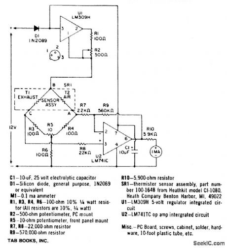
A bridge circuit contains two 100-ohm resistors (R3 and R4), and two thermistors (T1 and T2). At room temperature the resistance of T1 and T2 is about 2000 ohms. When they are each heated to 150℃ by a 10 mA current, the resistance value decreases to 100 ohms. Thus, the four elements comprise a bridge circuit. A characteristic of CO is that it conducts heat away from a thermistor at a different rate than air. One thermistor, T1, is exposed to the automobile exhaust while the other, T2, is isolated in a pure air environment. The difference in thermal conduction unbalances the bridge. A voltage difference is caused between points A and C. A differential amplifier, U1, amplifies this difference and drives the meter with sufficient current to read out the percentage of CO and the air-fuel ratio. A front panel balance control, R5, balances the bridge and calibrates the instrument. Calibration is performed when both thermistors are exposed to the outside air. (View)
View full Circuit Diagram | Comments | Reading(587)
Published:2009/7/2 4:49:00 Author:May
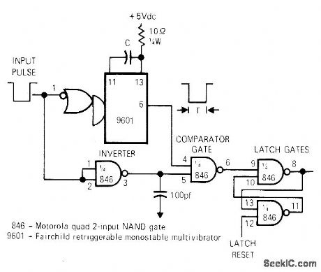
False triggering of latch gates by noise spikes is prevented by generating pulse T whose width is equal to minimum width of desired input pulse. Values used for RC combination set T. If R is chosen as 10 kilohms, C should be T/3.424, where C is in picofarads and T is in nanoseconds.-S. ft. Martin, Latching Circuit Provides Noise Immunity, EDN/EEE Magazine. Feb. 1. 1972. p 56. (View)
View full Circuit Diagram | Comments | Reading(519)
Published:2009/7/24 2:21:00 Author:Jessie

Fig. 13-15 This circuit is similar to that of Fig. 13-14, except that a type-K thermocouple subtracts from the LT1025 in series-opposed fashion. The net result is fed to the amplifier. Optional pull-down resistor R4 allows readings below 0℃. Linear Technology, Linear Applications Handbook 1990 p AN28-5. (View)
View full Circuit Diagram | Comments | Reading(619)
Published:2009/7/2 4:46:00 Author:May

Circuit Notes
To prevent loss of data when a CMOS RAM is switched from normal operation (VCC=5 volts) to stand-by mode (VCC=VgAT) it must be ensured that the CS pin goes near the VCC rail at all times. Ac coupling to the chip select is made through capacitor C, breaking the dc current path between Vgg (and hence VgAT) and the decoder output. So, whatever the impedance state of the decoder in power down, the battery will provide current only for the RAM, low enough to keep the voltage at CS near to VCC. (View)
View full Circuit Diagram | Comments | Reading(683)
Published:2009/7/2 4:46:00 Author:May
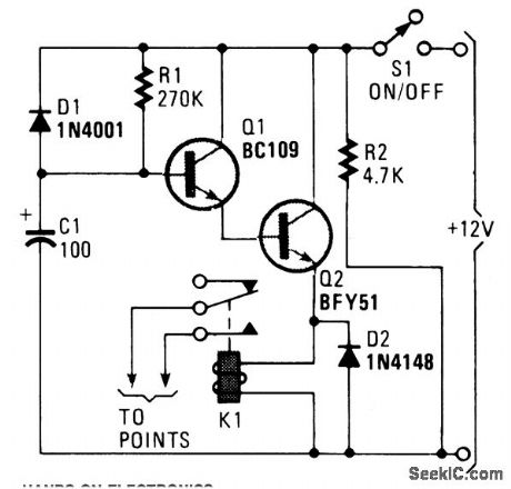
A flip of 51 puts the circuit into action. Power for the circuit is picked up from the ignition switch, and the circuit receives no power until the ignition switch is closed. When power is turned on, capacitor C1 is not charged and the emitter-follower Darlington pair (formed by Q1 and Q2) are cutoff, thus no power is applied to the relay (K1), which serves as Q1's emitter load. The relay's normally-open contacts are connected across the vehicle's points. (At this time, the relay contacts are open and have no effect on the ignition system). C1 charges by way of R1, causing the voltage at the base of Q1 to rise steadily. Thit creates a similar rise in the voltage at the emitter of Q2. A Darlington pair is used to provide a high input-impedance, buffer stage so that the voltage across C2 is free to rise almost to the full supply potential. Loading effects do not limit the charge potential to just a few volts. Eventually, the voltage applied to the relay becomes sufficient to activate it. The contacts close and short out the points. The ignition system now doesn't act properly and the vehicle is disabled. If the ignition is switched off, power is removed from the circuit and diode D1, which was previously reverse-biased, is now forward biased by the charge on C1. D1 allows C1 to rapidly discharge through R2 (and any other dc paths across the supply lines). The circuit is ready to operate when the ignition is again turned on. The engine will operate, but not for very long. The values of R1 and C1 provides a delay of about 25 to 30 seconds. Increase R1's value to provide a longer delay; (View)
View full Circuit Diagram | Comments | Reading(1427)
Published:2009/7/24 2:21:00 Author:Jessie

This circuit operates for a 6- or 9-V battery and provides 5-V output at 50 mA (even though the quiescent current is 40 μA). (View)
View full Circuit Diagram | Comments | Reading(699)
Published:2009/7/2 4:45:00 Author:May

The circuit provides a delayed windshield wiping, and dynamic braking of wiper blades when they reach the rest position. This prevents the blades from overshooting, which might cause them to stop at a point where they interfere with the drivers' vision.With the original wiper switch off, switch S1A turns on the delay circuit and S1B disconnects the original automotive wiring. When S1 is tumed off, the original wiring controls the system and the delay circuit is bypassed.Turning S1 on applies the + 12-V battery to U1 which is a voltage doubler that produces + 18 V. This higher voltage supply is necessary to ensure reliable turn on of Q1 by multivibrator U2. This arrangement provides about +18 V to the gate of Q1, whose source is +12 V minus the VDS drop of Q1.Q1 remains on for a time determined by the WIPES potentiometer. The interval between wipes is controlled by the PAUSE control. When C1 drops below +4 V, U2 ftres, tuming Q1 on and restarting the cycle. (View)
View full Circuit Diagram | Comments | Reading(1076)
Published:2009/7/24 2:20:00 Author:Jessie

Range is covered in four steps. Two-stage oscillator is followed by buffer that delivers 3.5 v to 2,000-ohm load.-V. Glover, Using a New Device: Field-Effect Transistor Oscillators, Electronics, 35:51, p 44-46. (View)
View full Circuit Diagram | Comments | Reading(605)
Published:2009/7/24 2:20:00 Author:Jessie

Control circuit uses gated rectifiers to generate welding pulses for rates up to 15 welds per second in foils up to 10 mils thick.-D. D. Kline, Automatic Welder for Thin Foils,Electronics,33:36,p 48:49. (View)
View full Circuit Diagram | Comments | Reading(654)
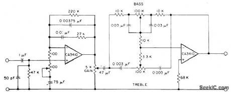
Published:2009/7/2 4:40:00 Author:May

The circuit shows a combination of balance and loudness controls. Due to the non-linearity of the human hearing system, the low frequencies must be boosted at low listening levels. Balance, level, and loudness controls provide all the listening controls to produce the desired music response. (View)
View full Circuit Diagram | Comments | Reading(1637)
Published:2009/7/24 2:20:00 Author:Jessie

Battery-operated fixed-frequency calibration source gives constant amplitude within 1% between 0 and 70℃, with less than 1% harmonic distortion. Circuit generates square wove, then converts if to sine wave in low-pass filter network. Frequency remains constunt at around 850 cps within 4% over operating temperature range.-Constant-Amplitude Sine-Wave Source, Electronic Circuit Design Handbook, Mactier Pub. Corp., N.Y, 1965, p 166. (View)
View full Circuit Diagram | Comments | Reading(654)
Published:2009/7/2 4:39:00 Author:May

This circuit should prove suitable as a design example for audio sound application. (View)
View full Circuit Diagram | Comments | Reading(581)
Published:2009/7/2 4:39:00 Author:May

Used to measure noise floor of receiver under test. RF source is simple, well-shielded crystal-controlled oscillator that is decoupled from battery supply. After attenuator resistors are adjusted to provide about S7 signal in receiver, oscillator housing is sealed with solder. Once calibrated, RF source is comparable to commercial signal generator, as leakage is quite low. Output is.-112 dBm at 14 MHz. L1 has 24 turns enamel on Amidon T5O-6 toroid. with 1 turn for output link.-W. Hayward. Defining and Measuring Receiver Dynamic Range. QST. July 1975. p 15-21 and 43. (View)
View full Circuit Diagram | Comments | Reading(895)
Published:2009/7/24 2:20:00 Author:Jessie
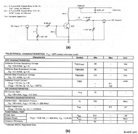
The electrical characteristics for the 2N3948 shown in this circuit are given in Fig. 2-15B. (View)
View full Circuit Diagram | Comments | Reading(582)
Published:2009/7/2 4:38:00 Author:May

A microphone preamplifier using a :om CM0S op amp complete with its own battery, is small enough to be put in a small mike case. The amplifier operates from a 1.5-V mercury cell battery at low supply currents. This preamplifier will operate at very low power levels and maintain a reasonable frequency response as well. The TLC251 operated in the low bias mode (operating at 1.5 V) draws a supply current of only 10 μA and has a -3 dB frequency response of 27 Hz to 4.8 kHz. With pin 8 grounded, which is designated as the high bias condition, the upper limit increases to 25 kHz. Supply current is only 30 μA under those conditions. (View)
View full Circuit Diagram | Comments | Reading(1013)
Published:2009/7/2 4:37:00 Author:May
This circuit has RIAA playback equalization, tone controls, and adequate gain to drive a majority of commercial power amplifiers, using the CA3410 BiMOS op amp. Total harmonic distortion, when driven to provide a 6-V output, is less than 0.035% in the audio-frequency range of 150 Hz to 40 kHz. Complete stereo preamplifier consists of duplicating this circuit using the two remaining CA3410 amplifiers. (View)
View full Circuit Diagram | Comments | Reading(728)
Published:2009/7/2 4:37:00 Author:May
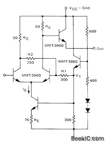
Motorola MMT3960 transistor array is connected as differential amplifier with feedback to produce Schmitt trigger having input hysteresis of 500 mV. Small rise and fall times make circuit suitable for driving flip-flop over wide range of frequencies.-B. Broeker, Micro-T Packaged Transistors for High Speed Logic Systems, Motorola, Phoenix, AZ, 1974, AN-536, p 6. (View)
View full Circuit Diagram | Comments | Reading(975)
Published:2009/7/2 4:36:00 Author:May
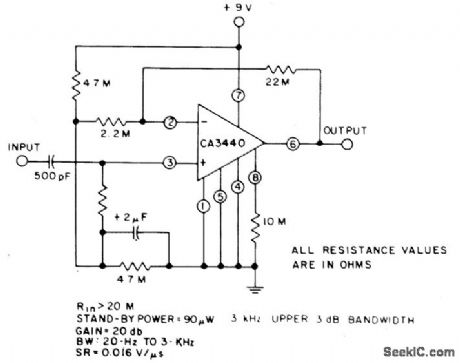
This circuit takes advantage of low power drain,high input impedance,and theexcellent frequency capability of the CA3440.Only a 500-pF input coupling capacitor is needed to achieve a 20 Hz, -3 dB low-frequency response. (View)
View full Circuit Diagram | Comments | Reading(511)
Published:2009/7/2 4:35:00 Author:May

A MC3340P is used as a variable gain amplifier. The output of TR2 is rectified and controls the gain of IC1. (View)
View full Circuit Diagram | Comments | Reading(1628)
| Pages:1148/2234 At 2011411142114311441145114611471148114911501151115211531154115511561157115811591160Under 20 |
Response in 12 hours
© 2008-2012 SeekIC.com Corp.All Rights Reserved.