
Circuit Diagram
Index 1173
10_MHz_fiberoptic_receiver_signal_conditioner
Published:2009/7/24 3:38:00 Author:Jessie

Fig. 14-10 This circuit accurately conditions a wide range of light-signal inputs at data rates up to 10 MHz. The circuit has both analog and digital outputs, as well as an analog output to monitor the detector. The digital output features an adaptive threshold trigger, which accommodates varying signal intensities (because of component aging, etc.). A test circuit is also included on Fig. 14-10. No calibration is required, Linear Technology Linear Applications Handbook 1990, p AN13-23.
(View)
View full Circuit Diagram | Comments | Reading(492)
FAST_800_V_SWEEP
Published:2009/7/24 3:38:00 Author:Jessie

Hybrid bootstrap or arangement with transistors in cascade generates 800-V sweeps in either polarity with 0.15 microsec duration.-F. Q. Creed, Hybrid Bootstrap Circuits Increase Sweep Linearity, Electronics, 34:31, p 46-48. (View)
View full Circuit Diagram | Comments | Reading(552)
SERIES_REGULATED_LINEAR_POWER_SUPPLY
Published:2009/7/24 3:37:00 Author:Jessie

The ac line is isolated from the power supply by transformer T1. Full-wave diode bridge BR1 de-livers unregulated dc with ripple on it to the filter capacitor (C1.) The filtered dc is delivered to pass transistor Q1, shown here in series with the load. The series-pass regulator with a transistor pass element regulates the voltage to ensure that a constant output level is maintained, despite variations in the power line voltage or circuit loading. The basic linear series regulator consists of transistor Q1, reference resistor R1, sensing resistors R2 and R3, voltage-reference zener diode D1, and operational amplifier IC1, organized as an error amplifier The zener diode D1 provides a fixed reference voltage at the positive input to amplifier IC1. The output voltage of the supply establishes the emitter volt-age and provides a feedback voltage for the negative terminal of the amplifier IC1, The equation for the regulated output voltage is Vreg=Vref(1+R1/R2) (View)
View full Circuit Diagram | Comments | Reading(986)
SCA_Background_Music_DECODER
Published:2009/7/1 20:37:00 Author:May

A resistive voltage divider is used to establish a bias voltage for the input (Pins 2 and 3). The demodulated (multiplex) FM signal is fed to the input through a two-stage high-pass filter, both to effect capacitive coupling and to attenuate the strong signal of the regular channel. A total signal amplitude, between 80 mV and 300 mV, is required at the input. Its source should have an impedance of less than 10,000 ohm. The Phase-Locked Loop is tuned to 67 kHz with a 5000 ohm potentiometer, only approximate tuning is required since the loop will seek the signal. The demodulated output (Pin 7) passes through a three-stage low-pass filter to provide de-emphasis and attenuate the high-frequency noise which often accompanies SCA transmission. Note that no capacitor is provided directly at Pin 7; thus, the circuit is operating as a first-order loop. The demodulated output signal is in the order of 50 mV and the frequency response extends to 7 kHz. (View)
View full Circuit Diagram | Comments | Reading(1544)
30_to_150_MHz_30_W_MOS_amplifier_28_V_supply
Published:2009/7/24 3:37:00 Author:Jessie
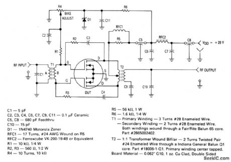
The electrical characteristics for the MRF136Y shown in this circuit are given in Fig. 2-2-48B. (View)
View full Circuit Diagram | Comments | Reading(444)
WHO_IS_FIRST
Published:2009/7/1 20:35:00 Author:May
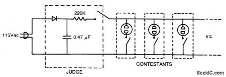
Circuit Notes
Here is a circuit for any question-and-answer party game. The first button pushed ionizes the neon bulb dropping the dc voltage on the parallel neons (the other contestants) below the ionization level: determining unequivocally the first person to press the button. (View)
View full Circuit Diagram | Comments | Reading(466)
Micropowover_inverting_switching_regulator
Published:2009/7/24 3:37:00 Author:Jessie

Figure 8-2 shows a MAX634 connected to provide -5-V, -9-V, -12-V, or -15-V outputs, depending on the value of R1. Figure 8-3 shows coil and core manufacturers. The input can be from +3V to +16.5 V, with 100 μA typical operating current and 85% efficiency. Nhxttvt NEW RELEASES DATA BOOK, 1992, P. 4-69, 4-70. (View)
View full Circuit Diagram | Comments | Reading(652)
ANALOG_MEMORY
Published:2009/7/1 20:35:00 Author:May
Used in synthesizer for generating wide variety of musical and other sounds, to provide constant control signal for sounds requiring long fadeout. Positive input pulse initiates sampling of analog signal for pre-set time, with signal being held for unspecified period. Input voltage range is from about -0.5 V to +6.5 V, being deliberately limited by D1 Three-part article describes operation in detail and gives all other circuits used in synthesizer.-T. 0rr and D. W. Thomas, Elec-tronic Sound Synthesizer, Wireless World, Part 3-Oct. 1973, p 485-490 (Part 1-Aug. 1973, p 366-372; Part 2-Sept. 1973, p 429-434). (View)
View full Circuit Diagram | Comments | Reading(661)
TRIGGERED_GROUNDED_GRID
Published:2009/7/24 3:37:00 Author:Jessie

Triggered linear sawtooth generator uses grounded-grid amplifier, eliminating initial step voltage that usually occurs in Miller sweep.-C. Sing, Grounded-Grid Circuit Sweeps Better Than Miller or Bootstrap, Electronics, 38;6, p 83-84. (View)
View full Circuit Diagram | Comments | Reading(553)
FREQUENCY_DIVISION_MULTIPLEX(FDM)STEREO_DECODER
Published:2009/7/1 20:33:00 Author:May
View full Circuit Diagram | Comments | Reading(2528)
Low_voltage_step_up_converter
Published:2009/7/24 3:37:00 Author:Jessie


This circuit shows a switching converter (chapter 4) that provides +5 V at 40 mA from one or two battery cells. Figure 8-42B shows the L2 inductor part numbers for a number of readily available batteries. (View)
View full Circuit Diagram | Comments | Reading(587)
TWO_TRANSISTOR_PHANTASTRON_SWEEP
Published:2009/7/24 3:36:00 Author:Jessie

Combined positive and negative feedback loops in two. transistor circuit give phantastron effect of single pentode with good sweep linearity.-A. S. Kislovsky, Sweep Circuits Using Two Three-Terminal Active Elements, Electronics, 35:12, p 54-55. (View)
View full Circuit Diagram | Comments | Reading(834)
Photodiode_signal_conditonerfrepuency_output
Published:2009/7/24 3:36:00 Author:Jessie
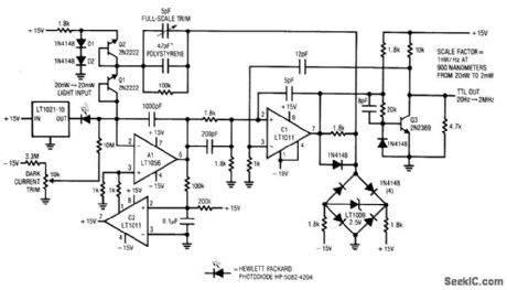
Fig. 14-9 This circuit converts a photodiode current output into an output frequency with 100 dB of dynamic range. Optical input power of 20 nW to 2 mW produces a linear 20-Hz to 2-MHz output. To calibrate the conditioner, place the photodiode in a completely dark environment and adjust the dark current trim so that the circuit oscillates at the lowest possible frequency, typically 1 or 2 Hz. Next, apply(or electrically simulate using the manufacturer's datasheet for light-input Versus output-current data)a 2-mW optical input. Adjust the full-scale trim capacitor for a 2-MHz output. If the adjustment is outside the range of the trimmer, alter the 47-pF value appropriately, Once calibrated, this circuit will maintain 1% accuracy(limited by the photodiode characteristics), Linear Technology Linea Applications Handbook 1990, p. AN7-9. (View)
View full Circuit Diagram | Comments | Reading(726)
TIME_DIVISION_MULTIPLEX(TDM)STEREO_DECODER
Published:2009/7/1 20:31:00 Author:May

View full Circuit Diagram | Comments | Reading(2493)
LOW_OUTPUT_FOR_POWER_ON
Published:2009/7/1 20:28:00 Author:May

Logic signal controls both turn-on and turnoff of 555 timer used as oscillator. When input signal at cathode of CR2 goes low, oscillator remains off and out-put at pin 3 is low. When input goes high, os-cillator starts with its first state low so there are no initial pulse errors.-K. D. Dighe, Rearranged Components Cut 555's Initial-Pulse Errors, EDN Magazine, Jan. 5, 1978, p 82 and 84 (View)
View full Circuit Diagram | Comments | Reading(580)
MICROPOWER_MONO
Published:2009/7/1 19:54:00 Author:May
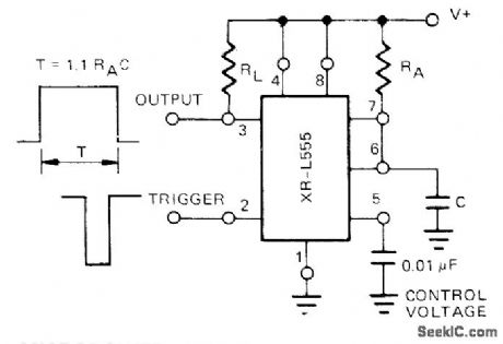
Uses Exar XR-L555 having typical power dissipation of only 900 μW at 5 V, serving as direct replacement for 555 timer in micropower circuits. Time delay is con-trolled by one external resistor and one capacitor (RA and C) which determine output pulse duration. Can be triggered or reset on falling waveform. Output will drive TTL circuits or source up to 50 mA.- Timer Data Book, Exar Integrated Systems, Sunnyvale, CA, 1978, p 7-8. (View)
View full Circuit Diagram | Comments | Reading(579)
SHF_SWEEP_GENERATOR
Published:2009/7/24 3:36:00 Author:Jessie

Swept-frequency signal source using backward-wove oscillator tube offers variable sweep rate in microwave region between 8,200 and 12,400 Mc. Sweep width is continually adjustable from 3 Mc to 4,200 Mc. May be modulated with either f-m or a-m.-D. E. Wheeler and P. D. Lacy, SHF Frequency Sweeper Uses Backward-Wave Tube, Electronics, 31:1, p 76-78. (View)
View full Circuit Diagram | Comments | Reading(742)
150_MHz_15_W_MOS_amplifier_28_V_supply
Published:2009/7/24 3:36:00 Author:Jessie
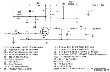
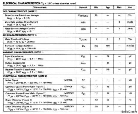
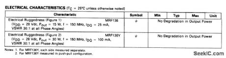
The electrical characteristics for the MRF136 shown in this circuit are given in Fig. 2-48B. (View)
View full Circuit Diagram | Comments | Reading(561)
HIGH_SPEED_HYBRID_BOOTSTRAP
Published:2009/7/24 3:35:00 Author:Jessie

Speed is increased because Cc does not have to supply charging current for Cs, but only current re quired by grid leak resistor; this is small, so Cc can be small und easily recharged during quiescent period.-F. C. Creed, Hybrid Bootstrap Circuits Increase Sweep linearity, Electronics, 34:31, p 46-48. (View)
View full Circuit Diagram | Comments | Reading(494)
Micropower_step_up_switching_regulator
Published:2009/7/24 3:35:00 Author:Jessie

Figure 8-1 shows a MAX630 connected to provide -15-V output at 20 mA. The input can be from 2.0 V to 16.5 V, with 70-μA typical operating current, 1-μA maximum quiescent current, and a 85% (typical) efficiency. MAXIM NEW RELEASES DATA Book, 1992, P. 4-49. (View)
View full Circuit Diagram | Comments | Reading(603)
| Pages:1173/2234 At 2011611162116311641165116611671168116911701171117211731174117511761177117811791180Under 20 |
Circuit Categories
power supply circuit
Amplifier Circuit
Basic Circuit
LED and Light Circuit
Sensor Circuit
Signal Processing
Electrical Equipment Circuit
Control Circuit
Remote Control Circuit
A/D-D/A Converter Circuit
Audio Circuit
Measuring and Test Circuit
Communication Circuit
Computer-Related Circuit
555 Circuit
Automotive Circuit
Repairing Circuit