
Circuit Diagram
Index 1179
BCD_DECODER_1
Published:2009/7/1 5:36:00 Author:May

Radio Shack RS7447 BCD to 7-segment decoder converts settings of four BCD input switches to corresponding 0-9 digit on 7-segment commonanode LED display. Display is Radio Shack 276-053. Battery can be four AA cells in series,with 1N914 diodeinserted in positive lead to reduce voltage to 5 v.-F.m.Mims, Integrated Cirouit Proieets, Vol 2, Radio Shack,Fort Worth,TX,1977,2nd Ed.p 27-40. (View)
View full Circuit Diagram | Comments | Reading(5509)
VARIABLE_PULSE_WIDTH
Published:2009/7/1 5:36:00 Author:May

R1 and C2 together provide wide range of pulse widths from Motorola MC851P mono. Rise and fall times of complementary output pulses are better than 100 μs. With only four switched capacitors in combination whh R1, pulse widths can be varied between maximum of 4.5 ms and minimum well under 4.5 μs.-C. W. Stoops, Wide-Range Variable Pulse-Width Monostable, EEE Maga-zine,.Dec. 1970, p 56. (View)
View full Circuit Diagram | Comments | Reading(733)
FREQUENCY_DOUBLING_TACHOMETER
Published:2009/7/1 5:35:00 Author:May

Connection shown for National LM2907 IC provides output pulse each time sine-wave input from magnetic pickup crosses zero, for use in digital control system. Width of each pulse is determined by size of C1 and supply voltage used.Circuit serves for doubling frequency presented to microprocessor control system.- Linear Applications, Vol. 2, National Semiconductor, Santa Clara, CA, 1976, AN-162, p12-13. (View)
View full Circuit Diagram | Comments | Reading(3254)
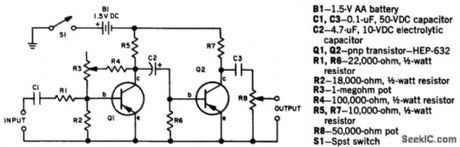
LOW_COST“HEADS_OR_TAILS”
Published:2009/7/1 5:33:00 Author:May

Circuit NotesS1 must be a push-to-make, release-to-break, switch. (View)
View full Circuit Diagram | Comments | Reading(453)
OUTBAND_DESCRAMBLER
Published:2009/7/1 5:32:00 Author:May

This circuit consists of an amplifier for the synch channel and a video detector which controls an attenuator so that the gain of the systems is increased during synch intervals. Kit available from North Country Radio, P.O. Box 53, Wykagyl Station, New York 10804. (View)
View full Circuit Diagram | Comments | Reading(1380)
POT_SHOT
Published:2009/7/1 5:31:00 Author:May
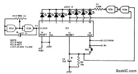
Circuit Notes
This is a circuit for a game of the shooting gallery variety. IC2a and b form an astable multivibrator clocking IC1 which causes LEDs 1-8 to flash in turn LED 5 is the target LED and the object of the game is to depress PBI just as LED 5 comes on. If this is done, the whole display is blanked for a few seconds signifying a hit. Otherwise, the LED which was lit remains lit. When the push button is released, C2 dis-charges through R2 taking 8 pin 13 low again and the LEDs will start to flash again. (View)
View full Circuit Diagram | Comments | Reading(827)
PWM_MONO
Published:2009/7/1 5:30:00 Author:May

Circuit provides pulse-width modulation with high duty cycles and comple-mentary output, Strobe input to gate G1 drives output of gate to binary 0, turning Q1 off and letting voltageacross C1 build up until UJT Q3 fires, discharging C1. Output of UJT drives output of G2 to binary 0. Article gives timing diagrams.-G. Lewis. Simple One Shot Has Complementary Outputs, EEEMagazine. Oct. 1970. p 78-79. (View)
View full Circuit Diagram | Comments | Reading(635)
FREQUENCY_INDICATOR_
Published:2009/7/1 5:29:00 Author:May

|Circuit furnishes green indication at resonance and red for either side of resonance. Uses Monsanto MV5491 dual redlgreen LED, with 220 ohms in upper lead to +5 V supply and 100 ohms in lower +5 V lead because red and green LEDs in parallel back-to-back have different voltage requirements. Useful for SSTV, RTTY, or subaudio-tone indication for control purposes on FM. Circuit requires two driver ICs and one section of hex inverter IC, with any suitable active filter used to form level detector for signals at desired frequency.-K.Powell, Novel Indicator Circuit, Ham Radio, April 1977, p 60-63. (View)
View full Circuit Diagram | Comments | Reading(729)
Quiescent_current_reduction_below_dropout
Published:2009/7/24 3:47:00 Author:Jessie

Figure 8-7 shows how the no-load quiescent current of the MAX667 (Figs. 8-5, 8-6) can be reduced to about 160 μA when the dropout voltage is reached. Notice that this circuit increases the dropout voltage by about 0.1 V MAXIM NEW RELEASES DATA BOOk, 1992, P. 4-138. (View)
View full Circuit Diagram | Comments | Reading(659)
FUZZ__BOX__1
Published:2009/7/1 5:26:00 Author:May

Circuit NotesThe input signal is amplified by the transistors. The distorted output is then clipped by the two diodes and the high frequency noise is filtered from the circuit via the 500 pF capacitor. The 1 M pot adjusts the intensity of the fuzz frog maximum to no fuzz (normal playing). (View)
View full Circuit Diagram | Comments | Reading(875)
GATE_DIPPER
Published:2009/7/1 5:24:00 Author:May


Used to determine resonant frequency of tuned circuit, provide signal for re-ceiver alignment, and make antenna measure-ments. Table gives winding data for plug-in coils L1. Parts values are not critical. T2 is tran-sistor interstage audio transformer with 10,000-ohm primary and 2,000-ohm secondary in meter circuit. JFET a1 is used in common-drain circuit followed by PNP bipolar transistor, with gate junction of JFET acting as rectifier. Dip meter M1 measures gate current, When tuned circuit of dipper is Ioaded by coupling it to extemal cir-cuit, power is absorbed and meter reads dip occurring when L1-C1 is tuned to resonance with external circuit. R1 is regeneration control.Audio amplifer 03-04 using 2N4125 or HEP52, optional, helps in Iistening to signals picked up by tuned circuit or enhances display on CROCan be used as field-strength meter if antenna is plugged into J1.-B. Clark, A Hybrid Gate-Dip Osdllator, QST, June 1974, p 33-37. (View)
View full Circuit Diagram | Comments | Reading(892)
PHANTASTRAN
Published:2009/7/24 3:47:00 Author:Jessie

Transistorized version phantastron eliminates voltage pedestal by connecting C2 directly to ground. Slope is independent of gain of Q4 and is varied by R4 ove, range of 100 to 1. Duty cycle can be up to 98%. R4 is 1,000 ohms and width control voltage is 0.4 V for ramp output shown.-G. Marosi, Novel Sweep Circuit Eliminates Romp Pedestal, Electronics, 38:26, p 68. (View)
View full Circuit Diagram | Comments | Reading(801)
POSITIVE_OUTPUT_MONO
Published:2009/7/1 5:23:00 Author:May
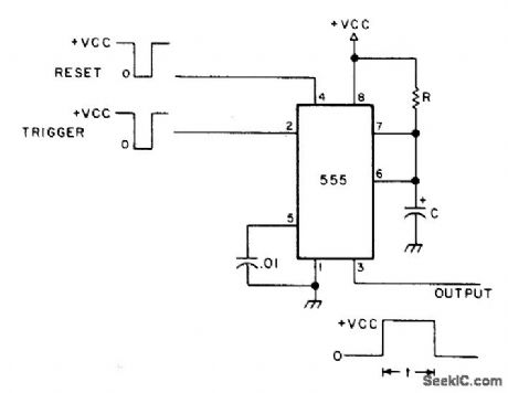
Timer is triggered by negative-going pulse to give positive output pulse whose width t in seconds is 1.1RC. VCC is 4.5-16 V at 3-10 mA.-H. M. Berlin, IC Timer Review, 73 Magazine, Jan. 1978, p 40-45. (View)
View full Circuit Diagram | Comments | Reading(696)
6_DIGIT_FOUR_FUNCTION
Published:2009/7/1 5:22:00 Author:May


National MM5777 calculator chip requires only keyboard, NSA1161 LED display, DS8977 digit driver, and 9-V battery to provide add, subtract, multiply, and divide functions. Calculator chip includes keyboard encoding and key debouncing circuits, along with all clock and timing generators. LED segments can be driven directly, without multiplexing. Seventh digit position is used for negative sign of 6-digit number and as error indicator.Leading and trailing zero suppressionis included.-, MOS/LSI Databook, National Semiconductor,Santa Clara,GA,1977,p 8-84-8-89. (View)
View full Circuit Diagram | Comments | Reading(1365)
Programmable_lozo_dropout_voltage_regulator
Published:2009/7/24 3:46:00 Author:Jessie

Figure 8-6 shows the MAX667 connected to provide a programmable output from +1.3 V to +16 V, with a low-battery function. Let R1 be 1 MΩ, and select R2 for a desired output using: R2= R1× (VOUT/VSET-1), where VSET= 1.225 V. Let R4 be 2.4 MΩ, and select R3 for a desired threshold of the low-battery detector using: R3=R4 ×(VBATT/VLBI-1). where VBATT is the desired threshold of the low-battery detector, and R3/R4 are the LBI input divider resistors. If VOUT is 5 V, a 5.5-V low-battery threshold can be set using 8.2 MΩ for R3 and 2.4 MΩ for R4. MAXIM NEW RELEASES DATA BOOk, 1992, p 4-137. (View)
View full Circuit Diagram | Comments | Reading(616)
BCD_DECODER
Published:2009/7/1 5:21:00 Author:May

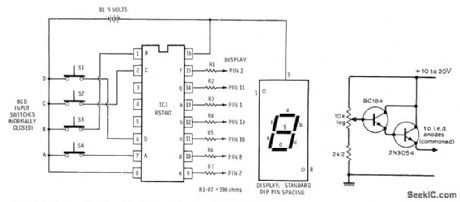
Radio Shack RS7447 BCD to 7-segment decoder converts settings of four BCD input switches to corresponding 0-9 digit on 7-segment commonanode LED display. Display is Radio Shack 276-053. Battery can be four AA cells in series,with 1N914 diodeinserted in positive lead to reduce voltage to 5 v.-F.m.Mims, Integrated Cirouit Proieets, Vol 2, Radio Shack,Fort Worth,TX,1977,2nd Ed.p 27-40. (View)
View full Circuit Diagram | Comments | Reading(3424)
001_Hz_to_7_MHz
Published:2009/7/1 5:20:00 Author:May
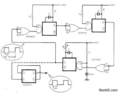
Generates square waves suitable for clock signals in sequential digital circuits, with values of RC pairs determining period in rangefrom about 150 ns to 120 s. To obtain equal mark-space ratio, set oscillator to half the required period and add bistable SN7474 divider as shown by dashed line,-P. J. Best, Monostable Ring Oscillator. Wireless World. March 1976. p 89. (View)
View full Circuit Diagram | Comments | Reading(683)
THREE_TRANSISTOR_PHANTASTRON
Published:2009/7/24 3:46:00 Author:Jessie

Use of both pnp and npn transistors gives desired current partition, while feedback required for sweep generator is provided by potentiometer arrangement at right.-N. C. Hekimian, Phantastron Circuits Using Transistors, Electronics, 34:8, p 46-47. (View)
View full Circuit Diagram | Comments | Reading(679)
Low_voltage_regulator
Published:2009/7/24 3:46:00 Author:Jessie

This circuit produces a 2-V output with a 3-V input. (View)
View full Circuit Diagram | Comments | Reading(679)
LOG_SWEEP
Published:2009/7/24 3:45:00 Author:Jessie
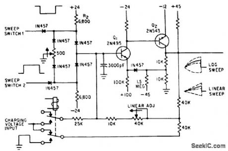
Resistance coupling in feed-back loop permits positive-going as well as negative-going waveforms. Circuit gives choice of logarithmic, exponential, or linear sweep output. Relay switches between linear and long sweep.-J. Curry and W. Sander, Bootstrap Generates Logarithmic Sweeps, Electronics, 33:52, p 60. (View)
View full Circuit Diagram | Comments | Reading(768)
| Pages:1179/2234 At 2011611162116311641165116611671168116911701171117211731174117511761177117811791180Under 20 |
Circuit Categories
power supply circuit
Amplifier Circuit
Basic Circuit
LED and Light Circuit
Sensor Circuit
Signal Processing
Electrical Equipment Circuit
Control Circuit
Remote Control Circuit
A/D-D/A Converter Circuit
Audio Circuit
Measuring and Test Circuit
Communication Circuit
Computer-Related Circuit
555 Circuit
Automotive Circuit
Repairing Circuit