
Circuit Diagram
Index 784
8_bit_parallel_adder_using_the_MC10181_
Published:2009/7/17 3:25:00 Author:Jessie

8-bit parallel adder using the MC10181 (courtesy Motorola Semiconductor Products Inc.). (View)
View full Circuit Diagram | Comments | Reading(2136)
RECEIVER_FRONT_END_RF_ATTENUATOR
Published:2009/7/17 3:24:00 Author:Jessie
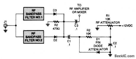
This PIN-diode front-end RF attenuator circuit contains a simple shunt circuit. The dc voltage from the potentiometer sets the attenuation level. The PIN diodes can be MV3404 or similar types. (View)
View full Circuit Diagram | Comments | Reading(1031)
ULTRASONIC_SOUND_SOURCE
Published:2009/7/11 2:04:00 Author:May
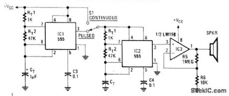
Using two NE555 timer IC devices, this circuit generates either pulsed or continuous ultrasonic signals. The sound frequency is:The values of CT for both pulse rate and ultrasonic frequencies can be calculated this way. SPKR is a small hi-ft tweeter. (View)
View full Circuit Diagram | Comments | Reading(645)
TRANSISTOR_STABILIZED_CMOS_FOUR_GATE_CLOCK
Published:2009/7/11 2:01:00 Author:May

Addition of 2N2222 transistor to clock using 4001 CMOS quad two-input NOR-gate IC boosts temperature stability to 0.05%/℃ and supply stability to 0.05%/V, Transistor circuit differentiates output signal of oscillator U1-U2 and provides pulses for toggling flipdlop U3-U4.-M. Eaton, Symmetrical.CMOS clock is inexpensive, EDN Magazine, March 20, 1974, p 80 and 83. (View)
View full Circuit Diagram | Comments | Reading(1090)
LOW_COST_BEACON_TRANSMITTER
Published:2009/7/11 2:01:00 Author:May

This transmitter uses a 48-MHz crystal oscillator to drive a diode tripler to the 144-MHz amplifier. The output is 5 to 10 mW. (View)
View full Circuit Diagram | Comments | Reading(1782)
32_bit_look_ahead_carry_adder_using_two_MC10179s_and_eight_MC10181_s
Published:2009/7/17 3:24:00 Author:Jessie

32-bit look-ahead carry adder using two MC10179s and eight MC10181 s(courtesy Motorola Semiconductor Products Inc.). (View)
View full Circuit Diagram | Comments | Reading(652)
LM317_REGULATOR_SENSING
Published:2009/7/17 3:24:00 Author:Jessie
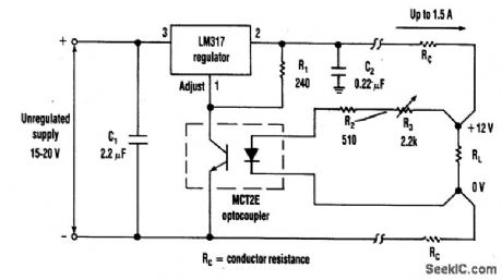
The optocoupler (as shown) provides load sensing for a 3-terminal regulator, such as the LM317 series. R1 sets a current of 5 mA through the optocoupler transistor and R3 is adjusted for 12 V across the load.
(View)
View full Circuit Diagram | Comments | Reading(3255)
80_AND_160_m_DIRECT_CONVERSION_RECEIVER
Published:2009/7/17 3:24:00 Author:Jessie
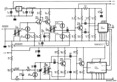

The full circuit diagram, except for power supply, for the direct-conversion top-band and 80-m receiver is shown. Incoming RF from the antenna is fed to the primary side of coil L1. This trans-former/coil is bought to resonance at the required frequency by a pair of back-to-back varicap diodes (VD1 and VD2). TRI, an RE, is coupled to the base (b) of transistor TR2, an emitter-follower. The output of TR2 feeds L2, the secondary being brought to resonance by varicaps VD3 and VD4. The variable-frequency oscillator (VFO) comprises a tuned circuit consisting of transformer L3, variable trimmer capacitor VC1, and varicap diode VD5. Variable bias to VD5 is provided by tuning control VR2. Transistor TR4 maintains oscillations at the desired frequency, and TR5 is an emitter-follower. The output of TR5 is sufficient to drive the CMOS divider chain formed by IC4. The VFO covers the frequency range 6.9 to 8.1 MHz, and this is divided by IC4 to produce 3450 to 4050 kHz for 80 m and 1725 to 2025 kHz for 160 m. The output of IC4 is fed to IC1, part of the product detector. The RF signal from the secondary tap on L2 is fed to a phase splitter formed around transistor TR3. Analog switch C1 operates at the selected VFO frequency and thus produces sum and difference frequencies of the VFO and the incoming RE. The output of IC1 at pin 4 is filtered to give resolved audio at this point. A high-gain inverting amplifier, with -3-dB points of approximately 300 Hz and 3 kHz, is formed by IC2a. This audio is now fed to IC3 with a maximum power output of 2 W. An LM380 is used in a standard configuration, and a fixed gain of around 30 dB is obtained. (View)
View full Circuit Diagram | Comments | Reading(1921)
SIGNAL_AVERAGER_CIRCUIT
Published:2009/7/17 3:24:00 Author:Jessie
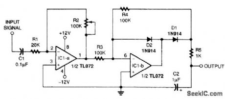
The first operational amplifier,IC1-a,is an inverthing amplifier whose gain can be adjusted up to 5.Adjustable feedback resistor R2 sets the circuit gain. The second amplifier,IC1-b,forms a half-wave rectifier and the signal averager clips the brief peaks and displays them over a longer period of time. (View)
View full Circuit Diagram | Comments | Reading(876)
MODEL_TRAIN_SOUNDER
Published:2009/7/17 3:23:00 Author:Jessie

This circuit can fit inside a model-train car and output any sound that you record in the ISD1000A,Imagine a cattle car that moos! The circuit can be used in model railroading to sound an electronic diesel horn when the train approaches a railroad crossing It is mounted on the bottom of the car When the sound car approaches the Crossing,S1 is momentarily closed by a magnet that must be installed under the track,starting the timing Cycle and sounding the horn Before you can use U2,the ISD1000A record and playback IC, you must first program it by breadboarding the circuit found In the applications data included with the IC To record sound on U2,you'll need a sample of the sound that you want the IC to play.The phone jack, which is mounted on the bottom of the car, serves two purposes It serves alb a means of charging B1, the 7 2-V NiCd battery, and it also provides a way to turn the circuit off. (View)
View full Circuit Diagram | Comments | Reading(3163)
Sinusoidal_VCO
Published:2009/7/17 3:23:00 Author:Jessie
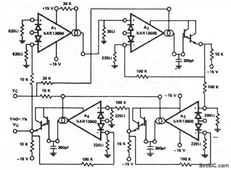
This circuit amplifiers configured as uses two XR-13600 OTAs (Fig.11-1B) , with three of the amplifiers configured as low-pass filters and the fourth as a limiter/inverter. The circuit oscillates at the frequency, where the loop phase-shift is 360° or 180°for the inverter and 60° per filter stage. This VCO operates from 5 Hz to 50 kHz with less than 1 % THD. EXAR corporation Databook, 1990 p 5-255 (View)
View full Circuit Diagram | Comments | Reading(776)
HIGH_OR_LOW_INPUT_REGULATOR
Published:2009/7/17 3:23:00 Author:Jessie

This regulator provides 12 V at 1 A out with an input voltage of 8 to 20 V. Output voltage can be changed by charging the 11-kΩ and 2.49-kΩ resistors to provide 2.21 V at the VFB pin of IC1, if desired. If you need to handle a higher input voltage, make sure to clamp the gate of Q1 below its 20-V max. rating.
Efficiency can exceed 70% for output currents greater than 0.5 A; above 15-V input voltage, more than 2 A of output current can be obtained. (View)
View full Circuit Diagram | Comments | Reading(1200)
VARIABLE_CURRENT_SOURCE0_TO_5A
Published:2009/7/17 3:23:00 Author:Jessie

The variable-current source generates 0 to 5 A with a compliance range of 4 to 30 V. The 12-bit digital-to-analog converter (DAC), IC2, makes it digitally programmable. The switch-mode step-down regulator, IC1, is more efficient than the alternative current source with linear pass transistor.IC3 is a high-side current-sense amplifier. In this circuit, it senses output current as a voltage drop across R5, and produces a proportional signal current at pin 8. The regulator's feedback voltage (IC1 at pin 1) is set by the DAC and modified by IC3's current feedback, which flows across a parallel combination of R2 and R3. This current feedback opposes any change in load current because of a change in load resistance. The DAC generates 0 to 10 V, producing a source current that varies inversely with code: FFFHEX (10 V from IC2) produces 0mA, and 000HEX (0V from IC2) produces 5 A. The circuit can be reconfigured for other ranges of output current (Isource) by resizing R2 and R3:
Isource=2217[VFB(R2+R3)-(R3VDAC)]/R2R3
where VFB 2.21 V and VDAC can range from 0 to 10 V.
The desired range for Isource defines values for R2 and R3:VDAC=10V for the low value of Isource and VDAC=0V for the high value of Isource. Substituting these two sets of values in the equation yields two equations to be solved simultaneously for the values of R2 and R3. (View)
View full Circuit Diagram | Comments | Reading(1653)
16_bit_look_ahead_carry_adder_using_an_MC10179_and_four_MC10181_s_
Published:2009/7/17 3:23:00 Author:Jessie

16-bit look-ahead carry adder using an MC10179 and four MC10181 s (courtesy Motorola Semiconductor Products Inc.). (View)
View full Circuit Diagram | Comments | Reading(588)
Ramp_pulse_VCO
Published:2009/7/17 3:22:00 Author:Jessie
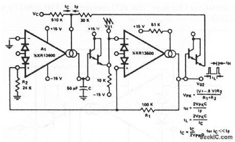
This circuit is similar to that of Fig. 11-13, except that the outputs are ramps and pulses. When V02 is high, IF is added to IC to increase the bias current of amplifier A1, and thus to increase the charging rate of capacitor C. When V02 is low, IF goes to zero and the capacitor discharge current is set by IC, EXAR Corporaton Databook 1990 p 5-255 (View)
View full Circuit Diagram | Comments | Reading(680)
NE602_MISER_CIRCUIT
Published:2009/7/17 3:20:00 Author:Jessie

This circuit uses an NE602 as a mixer in a typical application Component values depend on operating frequency and are typical for a 4 MHz operation Note that no IF filter is shown in the RE output circuit,A filter is necessary to select the desired output product and reject the others (View)
View full Circuit Diagram | Comments | Reading(1114)
EFFICIENT_NEGATIVE_VOLTAGE_REGULATION
Published:2009/7/17 3:20:00 Author:Jessie

Many applications require highly efficient negative-voltage post regulators with low dropout voltage in switch-mode supplies.
A way to provide good negattve-vottage regulation is with a low-dropout positive-voltage regulator operating from a well-isolated secondary winding of the switch-mode transformer. The technique works with any positive-voltage regulator, although highest efficiency occurs with low-dropout types.
In the circuit, two programming resistors, R1 and R2, set the output voltage to 12 V, and the LT1086s servo the voltage between the output and its adjusting (ADJ) terminals to 1.25 V. Capacitor C1 improves ripple rejection, and protection diode D1 eliminates common-load problems.
Because a secondary winding is galvanically isolated, a regulator's 12-V output can be referenced to ground. Therefore, in the case of a negative-voltage output, the positive-voltage terminal of the regulator connects to ground, and the -12-V output comes off the anode of D1. The Vin terminal floats at 1.5 V or more above ground. This arrangement is the equivalent of connecting the positive terminal of a battery to ground and taking the output from the negative terminal. (View)
View full Circuit Diagram | Comments | Reading(1051)
AM_BROADCAST_BAND_PRESELECTOR
Published:2009/7/17 3:19:00 Author:Jessie

The circuit for the AM-BCB preselector is completely bilateral; for that reason, J2 could just as easily be the input jack. That makes connecting the unit to your receiver a breeze. Note that switch S1 can be set so that the unit is bypassed. (View)
View full Circuit Diagram | Comments | Reading(1400)
Phase_sensitive_detector_for_sinusoidal_signals
Published:2009/7/17 3:19:00 Author:Jessie

Phase-sensitive detector for sinusoidal signals. This circuit measures the magnitude of in-phase or 180°-out-of-phase inputs with the proper polarity, depending on the relationship to the reference with less than 1% error. The op amp shown is a AD741J (courtesy Analog Devices, Inc.). (View)
View full Circuit Diagram | Comments | Reading(3580)
TWO_CHANNEL_AUDIO_MIXER
Published:2009/7/17 3:19:00 Author:Jessie

The figure shows a basic two-channel op-amp mixer circuit. The gain is equal to R5/R1 or R5/R2 for channel 1 or 2, respectively. Typically R1 and R2 are 2.2 to 22 kΩ and R5 is 10 to 100 kΩ, and the op amp is any suitable type, such as a 741 or its numerous variations. (View)
View full Circuit Diagram | Comments | Reading(3088)
| Pages:784/2234 At 20781782783784785786787788789790791792793794795796797798799800Under 20 |
Circuit Categories
power supply circuit
Amplifier Circuit
Basic Circuit
LED and Light Circuit
Sensor Circuit
Signal Processing
Electrical Equipment Circuit
Control Circuit
Remote Control Circuit
A/D-D/A Converter Circuit
Audio Circuit
Measuring and Test Circuit
Communication Circuit
Computer-Related Circuit
555 Circuit
Automotive Circuit
Repairing Circuit