
Circuit Diagram
Index 782
MODEL_RAILWAY_CROSSING_LIGHTS
Published:2009/7/17 3:34:00 Author:Jessie

The circuit is for use on model railway layouts and approximates the flashing light signals used at level crossings. It is operated by a reed switch (S1) embedded in the track, which is closed by a magnet on the underside of a passing train. This triggers the monostable timer IC1, which powers a Darlington transistor pair (TR1 and TR2). Diodes D1 and D2 (orange) illuminate, and also TR3 and TR4, connected as an astable, cause the red LEDs D3 to D6 to flash alternately for about 6 s, long enough for the train to pass. One set of LEDs is used on each side of the level crossing, for added realism. For 00 scale, 3-mm LEDs are best. (View)
View full Circuit Diagram | Comments | Reading(2810)
60_TO_72_MHz_VIDEO_AND_SOUND_RECEIVER_AND_IF_SYSTEM
Published:2009/7/17 3:34:00 Author:Jessie

This IF system uses a NE602 oscillator/mixer to convert VHF TV signals of 60 to 72 MHz (channe13 or channel4 under the U.S. NTSC) to 45 MHz. An SAW filter is used to provide bandpass filtering, followed by an LM1823 video IF/AGC/AFC/detector IC. Recovered video is fed to a sound trap and 4.5-MHz sound takeoff filter. Video is fed to the output emitter follower and is up to 1.5 V p-p into 75 Ω. An MC1357P FM IF/limiter/quadrature detector recovers audio information and provides 0.5 V p-p line-level audio. An LM555 oscillator and 1N914 diode act as a dc-to-dc converter system to derive a negative 3-V supply for the LM1823 AGC system. Both AFC and AGC voltages are available for interfacing with external down converters used for 440, 915, and 1280 MHz amateur TV reception. Operation is from a 12-V supply at about 200 mA.
A complete kit of parts, including PC board, is available from North Country Radio, P.O. Box 53, Wykagyl Station, New Rochelle, NY 10804-0053A. (View)
View full Circuit Diagram | Comments | Reading(2952)
Multiplexer
Published:2009/7/17 3:34:00 Author:Jessie
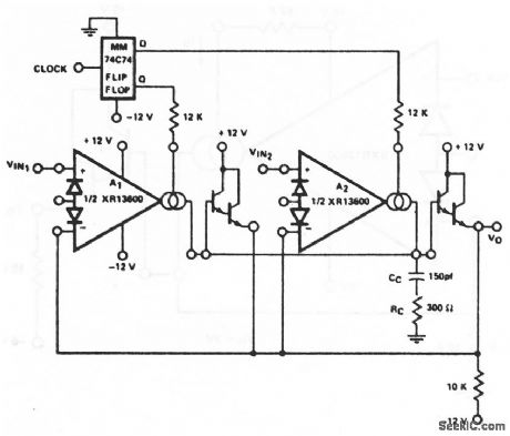
This circuit uses two sections of an XR-13600 (Fig.11-1B) and a standard flip-flop to form a multiplexer. The maximum clock rate is limited to about 200 kHz, with a maximum input differential of 5V. EXAS corporation Databook 1990 p 5-256 (View)
View full Circuit Diagram | Comments | Reading(859)
UJT_BISTABLE_WITH_DIODE_DECOUPLING
Published:2009/7/17 3:33:00 Author:Jessie
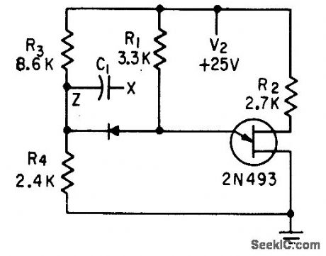
Needs only small negative trigger at X for turnoff.-T. P. Sylvan, Bistable Circuits Using Unijunction Transistors, Electronics, 31:51, p 89-91. (View)
View full Circuit Diagram | Comments | Reading(679)
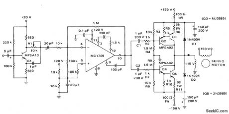
Servo_motor_preamplifier_1
Published:2009/7/17 3:32:00 Author:Jessie


Servo motor preamplifier(courtesy Motorola Semiconductor Products Inc.). (View)
View full Circuit Diagram | Comments | Reading(705)
13_V_AT_2_A_WITH_NPN_TRANSISTORS
Published:2009/7/17 3:32:00 Author:Jessie
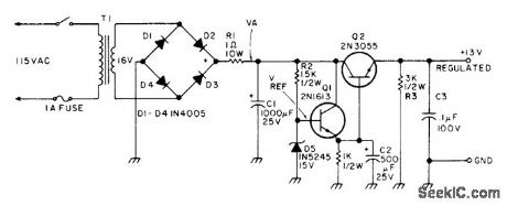
Q1 is reference voltage source and Q2 is series-pass regulator for basic supply suitable for running mobile FM transceiver or other 12-V portable equipment in home. Transformer secondary is 16-19 V, or can be 6-V and 12-V filament transformers in series. R1 protects rectifier diodes from surge current generated when supply is turned on. Article tells how to adapt circuit for other output voltages.-R. B. Joerger, Power Supply, 73 Magazine, Holiday issue 1976, p 40-41. (View)
View full Circuit Diagram | Comments | Reading(816)
BISTABLE_MAIN_GATE_MVBR
Published:2009/7/17 3:32:00 Author:Jessie
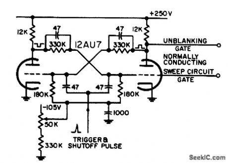
Provides positive unblanking gate. Used in radar to provide gates during which displayed sweep is generated, along with gates for waveforms that must be coincident with display sweep, but monostable mvbr is generally preferred for this application.-NBS, Handbook Preferred Circuits Navy Aeronautical Electronic Equipment, Vol. 1, Electron Tube Circuits, 1963, p N10-3. (View)
View full Circuit Diagram | Comments | Reading(595)
VARIABLE_VOLTAGE_REGULATOR
Published:2009/7/17 3:31:00 Author:Jessie

The op amp is wired as a×2 noninverting dc amplifier with a gam thatis determined by the R3/R2 ratio,The input voltage to the Op amp is variable between0 and 15 V via R5. The output voltage is therefore variable over the approximate range from 0.5 to 30 V The available output current has been boostedby adding transistor Q1 to the output. (View)
View full Circuit Diagram | Comments | Reading(0)
Servo_motor_preamplifier
Published:2009/7/17 3:30:00 Author:Jessie
Servo motor preamplifier (courtesy Motorola Semiconductor Products Inc.). (View)
View full Circuit Diagram | Comments | Reading(593)
HIGH_PERFORMANCE_VIDEO_MIXER
Published:2009/7/11 2:22:00 Author:May

This circuit mixes H synch. V synch. and actual video. T2 mixes the synch, while T1 serves as an emitter-follower. Bandwidths of up to 25 MHz are typical for this circuit. (View)
View full Circuit Diagram | Comments | Reading(1445)
PROGRAMMABLE_ZENER
Published:2009/7/17 3:30:00 Author:Jessie
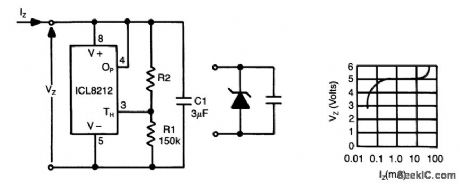
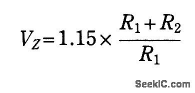
The ICL8212 is connected as a programmable zener diode,Zener voltages from 2 V up to 30 V can be programmed by suitably selecting R2.The zener voltage is∶
Because of the absence of internal compensation h the ICL8212,C1 is necessary to ensure stability.Two points worthy of note are the extremely low-knee current(less than 300 μA)and the low dynamic impedance (typically 4 to 7 ohms)over the operating current range of 300 μA to 12 mA. (View)
View full Circuit Diagram | Comments | Reading(1221)
MODEL_SPORTS_CAR_LIGHTING_SYSTEM
Published:2009/7/17 3:30:00 Author:Jessie

In order to add some realism to a model sports car, this simple circuit can be built into virtually any type of toy car, battery-operated or not. The design uses a CD4020 14-stage binary counter to operate LED tum indicators (D5 to D8), taillights (D9 and D10), and headlights (D11 and D12). The counter IC1 is clocked by a unijunction oscillator based around TR1. The red taillights and the yellow headlights draw a small current, supplied constantly by resistors R7 and R8. For added re-alism, this current is supplemented through resistors R1 and R2 to give an impression of headlights dipping and taillights braking. The model's turn indicators flash whenever they are enabled, and so the cathodes (k) of D5 to D8 are taken to another output (Q3, pin 7) of IC1. With their anodes (a) taken positive via resistors R3/R4 and the relevant counter output, they flash at the rate determined by Q3. The result is that one set of indicator lights flashes, then the other set, followed by both. The circuit is powered by a PP3-type or MN1604 9-V battery, and a small slide switch S1 can be mounted on the vehicle's underside. (View)
View full Circuit Diagram | Comments | Reading(4811)
Line_operated_servo_motor_amplifier
Published:2009/7/17 3:29:00 Author:Jessie
Line-operated servo motor amplifier (courtesy Motorola Semiconductor Products Inc.). (View)
View full Circuit Diagram | Comments | Reading(1725)
TIMER_FOR_CODE_PRACTICE
Published:2009/7/11 2:21:00 Author:May

Signetics NE555V timer operating on 9-V supply serves as AF oscillator providing adequate volume for classroom instruction. Output tone can be varied from several hundred to several thousand hertz.-J. Bumey, Code Practice Oscillator, OST, July 1974, p 37. (View)
View full Circuit Diagram | Comments | Reading(863)
SIMPLE_TRF_RECEIVER
Published:2009/7/17 3:29:00 Author:Jessie

Here is a receiver that contains an RF amplifier. The desired radio-frequency signal can be selected by tuning C5. (View)
View full Circuit Diagram | Comments | Reading(2102)
KEYER
Published:2009/7/11 2:20:00 Author:May

Uses gating and flip-flop functions to generate dots and dashes under control of gated clock. SN7413 Schmitt trigger is connected as relaxation oscillator. Circuit provides minimum spacing between dots and dashes re gardless of paddle movements.-A. D. Helf rick, A Simple IC Keyer, 73 Magazine, Dec. 1973, p 37-38. (View)
View full Circuit Diagram | Comments | Reading(5847)
REGULATOR_CIRCUIT
Published:2009/7/17 3:29:00 Author:Jessie
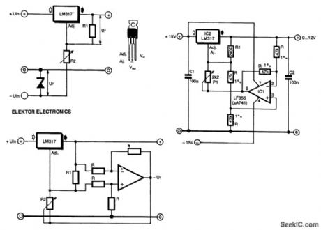
The special characteristic of this regulator is that the output voltage can be adjusted down to0 V. The regulation is provided by'an integrated regulator Type LM317. As is normal in supplies that can be adjusted to 0 V, this IC is used in conjunction with a zener diode. This diode provides a reference voltage that is equal, but of opposite sign, to the reference voltage (Ur) of the regulator, as shown in Fig. 74-1(a). Potential divider R1/R2 enables the output voltage to be adjusted.
In this circuit, the negative reference voltage is derived in a different manner: from the regulator with the aid of an op amp (Fig. 74-1(b)). The op amp is connected as a differential amplifier that measure, the voltage across R1 and inverts this voltage to Ur. An additional advantage of this method is that at low-output voltages, a change in the reference voltage has less effect on the output voltage than the circuit in Fig. 74-1(a). The prototype, constructed as shown in Fig. 74-1(c), gave very satisfactory results.
The op amp need not meet any special requirements: a μA741 works fine, although an LF356 gives a slightly better performance. The negative supply for the op amp can be obtained with the aid of a centertapped mains transformer. (View)
View full Circuit Diagram | Comments | Reading(751)
ANALOG_VOLTAGE_CAMERA_IMAGE_TRACKER
Published:2009/7/11 2:20:00 Author:May
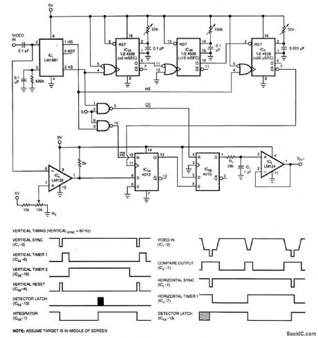
By using a low-cost RS-170 camera and this circuit, a voltage that trades the position of an object in the field of view of a camera is generated. IC2A and IC2B form a valid video gate that holds IC3 in reset during the internal vertical blanking to prevent false interpretation of the UB1 as black video. IC4 is a black level detector. The circuit tests for a black object in the middle of each video line. IC5 latches the comparator's output and produces a square wave whose duty cycle depends on where the black level is detected in the video field. R1. C1. and IC6 integrate and buffer the analog output voltage. (View)
View full Circuit Diagram | Comments | Reading(1086)
PWM_MODEL_RAILROAD_CONTROLLER
Published:2009/7/17 3:28:00 Author:Jessie

The PWM model train controller shown offers results that are far superior to those of a traditional rheostat-type model train controller and provides better fine control of train speeds. A 555 timer chip (IC1) is configured as a free-running oscillator operating at 80 kHz. The exponential ramp waveform generated across capacitor C3 feeds a comparator (IC2), whose threshold reference is set by logarithmic potentiometer VR1. The output of comparator IC2 is inverted by IC3a and IC3b and it drives the output stage, which comprises transistors TR1 and TR2; the latter can handle 2 A and dissipate 1 W, which is more than adequate for a saturated switch operation. Diode D2 protects against back BMP in the train motor. Short-circuit protection is provided with a 0.5-Ω series sense resistor (R8/R9). Transistor TR3 switches on when the current flowing reaches approximately 1.2 A. This sets the out-put of an S-R flip-flop (IC3c/lC3d) low. LED D3 illuminates to indicate a fault, and TR1 is disabled by the inverters. Capacitor C4 introduces a short time period across TR3 to prevent the cutout from triggering falsely. Push-switch S1 is a kick button. Pressing this causes a short, higher-voltage burst to be applied to reluctant motors. (View)
View full Circuit Diagram | Comments | Reading(6946)
CLOCK_OSCILLATOR
Published:2009/7/11 2:18:00 Author:May

Q11 and Q2 form oscillator section of tim-base generator, and Q3-Q4 serve as pulse shaper. Q1 is grounded-base voltage amplifier with tuned collector load.Q2 matches impedance of Q1 collector circuit to crystal. Output amplitude is limited by zener diode D1-R.S. Reed,Rugged Arming-Fuzing Timer for Atomic Artillery Mssile Electronics,34:38,p48-51. (View)
View full Circuit Diagram | Comments | Reading(824)
| Pages:782/2234 At 20781782783784785786787788789790791792793794795796797798799800Under 20 |
Circuit Categories
power supply circuit
Amplifier Circuit
Basic Circuit
LED and Light Circuit
Sensor Circuit
Signal Processing
Electrical Equipment Circuit
Control Circuit
Remote Control Circuit
A/D-D/A Converter Circuit
Audio Circuit
Measuring and Test Circuit
Communication Circuit
Computer-Related Circuit
555 Circuit
Automotive Circuit
Repairing Circuit