
Circuit Diagram
Index 787
TWO_PHASE_CLOCK_FOR_8080_1
Published:2009/7/11 1:43:00 Author:May

Typical clock design for Intel 8080 microprocessor system uses carefully designed logic sequence and level translation in combination with 32-MHz crystal to generate two-phase 12-V clock waveform.-S. G. Brannan, μP Clock Generators-Buy or Build? EDN Magazine,Sept 20,1975,p 53-55. (View)
View full Circuit Diagram | Comments | Reading(2384)
MATCHING_OPAMPS
Published:2009/7/11 1:43:00 Author:May
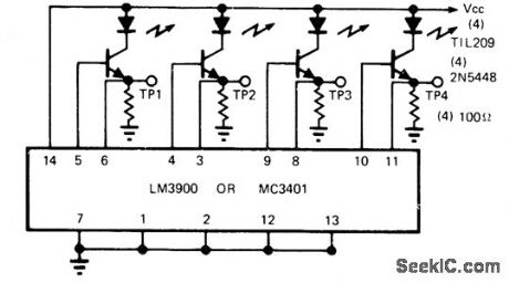
Simple circuit checks condition of quad Norton opamps (Nationai LM3900 or Motorola MC3401). Can also be used to match or select devices for similar DC characteristics in critical applications. Amplifier under test is plugged into socket connected as shown. Good unit makes all four LEDs glow with about same brightness, and all four testpoint voltages will agree within about 2 mV. If one section of amplifier is damaged, associated LED will glow very brightly or not at all. Wide variations between test-point voltages indicate partial damage. For critical applications, select amplifiers by matching average test-point voltages.-R. Tenny, Check Norton Amplifiers Quickly, EDNMagazine, March 5, 1974, p 72. (View)
View full Circuit Diagram | Comments | Reading(846)
SSB_COHERENT_RADAR_OSCILLATOR
Published:2009/7/17 3:07:00 Author:Jessie


Phase information of each transmitted pulse is stored in coherent oscillator V3 for use as reference voltage for analyzing doppler return from targets. Other stages are amplifiers. Oscillator lank is L1-C1-C2. This oscillator has good free-running stability and is easily locked in phase with 30.Mc input pulse.-J. B. Theiss, More Target Data with Sideband Coherent Radar, Electronics, 36:3, p 40-43. (View)
View full Circuit Diagram | Comments | Reading(920)
TWO_SPEED_CLOCK
Published:2009/7/11 1:42:00 Author:May

Creates alternative slow clock cycle for MOS Technology 6502 processor on KIM-1 microcomputer card under eontrol of SPEED SELECT line generated by slow memories. Control logic of 0 gives fast cycles, while logic 1 gives slow cycles. Processor cycle is maintained for 1 ps for fast memory access, but cycle is automatically stretched to 2μs for slower 2102s.-Y. M. Gupta, True Confessions: How I Relate to KIM, BYTE, Aug. 1976, p 41-48. (View)
View full Circuit Diagram | Comments | Reading(887)
TRANSlSTOR_TESTlNG_OSClLLATOR
Published:2009/7/11 1:41:00 Author:May

With any good general-purpose transistor, circuit delivers steady AF tone to earphone. To test another transistor, substitute it in appropriate socket. No tone means it is bad. Low tone or chirp indicates questionable condition. If type (PNP or NPN) is unknown, try in both sockets. If leads of unknown cannot be identified, try all three possible positions in socket.-Circuits, 73 Magazine, July 1977, p 35. (View)
View full Circuit Diagram | Comments | Reading(641)
DEEP_OCEAN_VELOCIMETER
Published:2009/7/17 3:07:00 Author:Jessie

Sonic pulse produced by transducer s is sent along fixedlength water path at any depth and picked up by receiving transducer R. Received signal is then amplified and fed back to blocking oscillator to synchronize it at repetition rate determined by delay time of pulse in water. Pulses then go to cable-driving circuit, and through cable to surface vessel for counting.-L. Dulberger, Deep-Ocean Velocimeter Aids Sonar Systems Design, Electronics, 34:22, p 41-43. (View)
View full Circuit Diagram | Comments | Reading(591)
TWO_INVERTER_COLPITTS
Published:2009/7/11 1:40:00 Author:May

Simpie low-cost clock uses two inverters in LC circuit. G1 operates as Colpitts oscillator, with C1 setting feed-back Ievel and L1-C2 setting frequency. Low DC resistance path through R1, R2, and L1 provides high negative DC feedback around G1 and biases it into Iinear region. G2 squares output of G1 to appropriate TTL levels. For values shown, output period is 1.2 μs and rise and fall times are under 20 ns.-C. A. Herbst, TTL Inverter Makes Stable Colpitts Oscillator, EDN|EEE Magazine, May 15, 1971, p 50. (View)
View full Circuit Diagram | Comments | Reading(1687)
Long_term_precision_integrator_for_such_applications_as_pollution_control
Published:2009/7/17 3:06:00 Author:Jessie

Long-term precision integrator for such applications as pollution control. The analog signal is applied to precision amplifier model 52K, then to the V/F converter input. Model 452's output is connected to a high capacity counter and display operating as a totalizer. The total pulse is equal to the time integral of the analog input (courtesy Analog Devices, Inc.). (View)
View full Circuit Diagram | Comments | Reading(1103)
2_m_TRANSMITTER
Published:2009/7/11 1:40:00 Author:May

The transmitter was designed specifically for use by radio amateurs as a radio beacon. As such, it provides a good-quality signal that is free of unwanted harmonics.Transistor T1, in association with crystal X1, operates as a 36-MHz oscillator. Filter L1/C3 obviates any tendency of the circuit to oscillate at 12 MHz (the fundamental frequency of the crystal).Circuit L2/C4 is tuned to the fourth harmonic of the oscillator signal (144 MHz). This signal is fed to the aerial via a buffer stage that consists of T2, a double-gated FET. The (amplitude) modulating signal is applied to the second gate of the buffer. The output power of the transmitter has been kept low, about 10 to 40 mW.The modulating signal is generated by N1, an oscillator that switches the transmitter on and off via transistor T3. The switching rate lies between 0.1 and 0.5 Hz. When the output of N1 is low, T3 is switched off, and the transmitter is inoperative because the supply is disabled. When the output of N1 is high, T3 is on and the transmitter operates normally.The digital pattern at the gate of T2 shapes the modulating signal. Gate N2 generates a square wave at afrequency of0.1 to 1 Hz. As long as the output of T3 is high, N4 oscillates atafrequency ofabout 1 kHz. At the relevant gate of N2, there is, therefore, a periodic burst-signal at 1 kHz, and this signal is used to modulate the transmitter.The digital pattern at the relevant gate of T2 can be varied to individual requirements by altering the values of the feedback resistors in the digital chain. The transmitter is calibrated by setting trimmers C4, C7, and C8 for maximum output power.Inductors L2 and L3 are wound from 0.8-mm diameter enamelled copper wire: L2 =5 turns with a tap of 1 turn from ground; L3A=3 turns and L3B=2 turns. The coupling between L3A and L3B should be arranged for maximum output power. The circuit draws a current of only 20 mA, which enables the trans-mitter to be operated from a 9-Y battery for several hours. (View)
View full Circuit Diagram | Comments | Reading(1645)
Voltage_controlled_resistor_with_linearizing_diodes
Published:2009/7/17 3:06:00 Author:Jessie

This circuit is essentially the same as that of Fig. 11-6, except that the linearizing diodes are included to improve noise performance of the resistor . EXAB Corporation Databook, 1990, p 5254 (View)
View full Circuit Diagram | Comments | Reading(629)
SIGNAL_INJECTOR
Published:2009/7/11 1:40:00 Author:May

Circuit is basically 1-kHz MVBR having high harmonic output through 50 MHz. Used with signal tracer for troubleshooting audio equipment. Practically any NPN transistors can be used Article gives troubleshooting techniques for all types of equipment.-M,James,Basic Troubleshooting,Ham Radio,Jan,1976, p54-57. (View)
View full Circuit Diagram | Comments | Reading(0)
SIMPLE_225_TO_400_MHz_AIR_BAND_RECEIVER
Published:2009/7/17 3:06:00 Author:Jessie

Tuning coil L2 can be wound with 2 turns of #22 wire on a 5/32 drill bit. This circuit is well behaved as long as a good component layout is used. The component leads must be kept short and neat, especially the leads of the transistor. The lengths should not exceed 3/16 . Audio could be tapped off the tuning coil with a 5-μF (or so) electrolytic capacitor, but the 1N82 diode circuit seems to produce less signal loss. The, RF signal from ANT1, an approximately 18 antenna, can be introduced through a small capacitor of 1 pF (or less) to the emitter of the 2N918. Other high-frequency transistors can be used, but might require different resistance in the regeneration circuit. The output of this circuit must go to an audio amplifier. (View)
View full Circuit Diagram | Comments | Reading(4808)
PULSE_ENERGY_ERGMETER
Published:2009/7/17 3:06:00 Author:Jessie

Bolometer bridge converts input signal to heat by integrating input power with respect to time. Heat upsets bridge balance, and resulting signal is amplified and applied to peak-holding voltmeter that indicates energy directly. Used to measure energy content of pulses.-L. A. Rosenthal, Ergmeter Measures Bursts of Energy, Electronics, 31:23, p 79-81. (View)
View full Circuit Diagram | Comments | Reading(605)
AMATEUR_TELEVISION_TRANSMITTER
Published:2009/7/11 1:37:00 Author:May

Although the unit was designed for 2 W operation, Q6 and Q7 stages and associated components can be omitted and about 1 to 30 mW of RE can be obtained by link coupling to L9. A complete set of parts, including PC board is available from North Country Radio, P.O.Box 53, Wykagyl Station, New Rochelle, NY 10804. (View)
View full Circuit Diagram | Comments | Reading(1782)
MEGAPULSE_GENERATOR
Published:2009/7/11 1:36:00 Author:May

Provides up to 18-Mc pulses for dynamic testing of high-speed digital computers. Can be used as clocking system. Major frequency changes in self-biased Hartley osdllcnor V6 are made with plug-in coilsll,and changes with C4.Positive output pulses,continuously variable between 0 and 20v,are generated in four output channels,in 10-microses or with 0 to 10 microsec blanks between strings of pulses when gated by pulse generator.-RW.Buchanan and B.Kautz,Dynamic Testing of Computer Building Block,Electronics,32:33,p66-68. (View)
View full Circuit Diagram | Comments | Reading(843)
TWO_PHASE_CLOCK_FOR_8080
Published:2009/7/11 1:34:00 Author:May


Crystal oscillator opetating at twice desired dock frequency uses pi network R1-C1-X1-C2 providing 180°phase shift required for positive feedback to input of oscillator G1. D flip-flop FF1 in divide-by-2 configuration generates one phase, while NOR gate G2 generates other phase from basic oscillator by masking out every other cycle. G3 merely provides enough propagation delay on second phase to prevent overlap with first phase. Crystal should be below 3 MHz.-D. M.Risch, 8080 CMOS Clock Uses Two IC's, EDN Magazine, Jan. 5, 1977, p 50. (View)
View full Circuit Diagram | Comments | Reading(2137)
SWITCHING_IMPROVES_REGULATOR_EFFICIENCY
Published:2009/7/17 3:05:00 Author:Jessie

In this circuit, a full-wave bridge is switched to a full-wale center tap to reduce regulator dissipation. SCR D6 switches between cottfieuraUons, When D6 is off, the circuit is an circuit is an FWCT rectifier using D1, D2, and D5, It applies 17 Vplus ripple to the regulator Input. The dron across the regulator supplies base driveto Q2. If Q2 is on, Q1 is off, and D6 is off. If the regulator voltage drops below about 3 V, Q2 turns off, and turns Q1 on, which turns on D6. This changes the circuit to an FW bridge USlng D1 through D4. (View)
View full Circuit Diagram | Comments | Reading(874)
CRYSTAL_CONTROLLED_MVBR
Published:2009/7/11 1:34:00 Author:May

Simplicity and stability make circuit useful as system clock.Will oscillate at 1 Mc over supply voltage range of 2 to 30v.Output is rounded square wave,at any frequency from 3 kc to 10 Mc depending on crystal used.-J. Freeman, Crystal Controlled Multivibrator, EEE,13:6, p65. (View)
View full Circuit Diagram | Comments | Reading(693)
Simple_integrator_using_an_ECG941_941D_941M_operational_amplifier
Published:2009/7/17 3:05:00 Author:Jessie

Simple integrator using an ECG941/941D/941M operational amplifier. Typical supply voltage is ±15 volts (courtesy GTE Sylvania Incorporated). (View)
View full Circuit Diagram | Comments | Reading(566)
CLOCK_PULSE_AMPlJFlER
Published:2009/7/11 1:33:00 Author:May
Genercates clock pulses for driving all flip-flops in magnetic drum timing channel system, and generates digit square-wave signals used in Manchester conversion network of writing amplifer. External signal generator provides desired frequency for time track.-A.j. Strassman and R.E. Keeter, Clock Track Recorder For Memory Drum, Electronics, 32:41, p74-76. (View)
View full Circuit Diagram | Comments | Reading(609)
| Pages:787/2234 At 20781782783784785786787788789790791792793794795796797798799800Under 20 |
Circuit Categories
power supply circuit
Amplifier Circuit
Basic Circuit
LED and Light Circuit
Sensor Circuit
Signal Processing
Electrical Equipment Circuit
Control Circuit
Remote Control Circuit
A/D-D/A Converter Circuit
Audio Circuit
Measuring and Test Circuit
Communication Circuit
Computer-Related Circuit
555 Circuit
Automotive Circuit
Repairing Circuit