
Circuit Diagram
Index 786
MMIC_AMPLIFIER_MIXER
Published:2009/7/17 3:11:00 Author:Jessie

This figures shows a simple mixer using an MMIC amplifier (View)
View full Circuit Diagram | Comments | Reading(638)
DIRECT_CONVERSION_WWV_RECEIVER
Published:2009/7/17 3:10:00 Author:Jessie
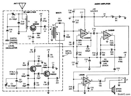
Incoming RF is picked by the antenna (ANTI) and is coupled via an autotransformer to a grounded-base amplifier (Q3) before being applied to a diode-mixer network that comprises T2, D1, and D2. The best mixer performance is obtained when both secondary windings of T2 are identical, and D1 and D2 are matched. The output of the local oscillator (LO)-a grounded-collector Colpitts oscillator (built around Q1)-is applied to emitter-follower/buffer Q2, which provides a low-impedance drive signal for the mixer. The demodulated signal is coupled to a pair of high-gain op-amp stages (U1-a and U1-b). The op amps provide a 50-dB gain. Amplifier U2 provides a 20-dB gain, thereby producing sufficient output drive for an 8-Ω speaker or 32-Ω headphones. The volume is controlled merely by adjusting the length of the whip antenna. When driving 32-Ω headphones, the circuit consumes less than 25 mA; however, the current drain increases to 40 mA when driving an 8-Ω speaker. (View)
View full Circuit Diagram | Comments | Reading(1131)
VTR_CLOCK
Published:2009/7/11 1:58:00 Author:May
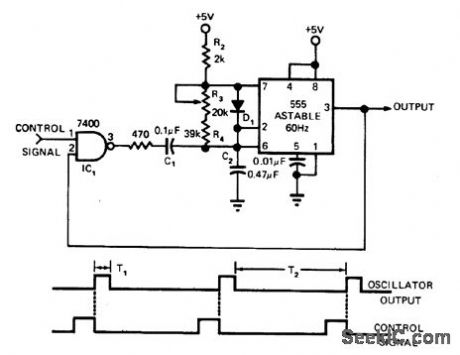
Locked oscillator using only two-input NAND gate and 555 timer provides logic clock signal for videotape recorder. Vertical sync signal, stripped from video information re corded on tape, is used as control signal. C1 controls locking range forfree running trequency of 555. When C2 is charging (555 output is high), R2 and D1 determine time constant T1. During discharge of C2, D1 is reverse-biased and discharge time constant T2 is determined by R3 and R4. -L. Saunders, Locked Oscillator Uses a 555 Timer, EDN Magazine, June 20, 1975, p 114. (View)
View full Circuit Diagram | Comments | Reading(713)
Voltage_controlled_low_pass_filter
Published:2009/7/17 3:10:00 Author:Jessie

This circuit performs as a unity-gain buffer amplifier at frequencies below cutoff, with the cutoff frequency being the point at which XC/gm equals the closed-loop gain of (R/RA). At frequencies above cutoff, the circuit provides a single RC rolloff (6 dB per octave) of the input signal with a -3-dB point that is defined by the given equation, where gm (of the XR-13600, Fig. 11-1B) is 19.2× IB at room temperature. EXAR Corporaton Databk 1990, p 5-254. (View)
View full Circuit Diagram | Comments | Reading(1475)
PROGRAMMABLE_IC_TESTER
Published:2009/7/11 1:57:00 Author:May

Provides automatic, instantaneous, and exhaustive tests of most small-scale integration gates, inverters, flip-flops, etc, and medium-scale integration counters, latches, shift registers, etc. Circuit sends eight lines of input data to device under test (DUT) and receives six lines of output. When TEST switch is closed, binary counter driving DUT input lines is cleared and flip-flop driving GO/NO-GO light is set. Upon release of switch, counter increments through all 256 input conditions. Between counts, data on output lines is compared with data stored in memories IC9-IC14. If mismatch exists, GO/NO-GO flip-flop is cleared at terminal count, CLEAR input of clock oscillator flip-flop is driven low, and further counts are inhibited until TEST button is pushed again. If GO/NO-GO light stays on, component passes test. To program, hold PROGRAM button down while testing known good device. Article gives examples of various applications.-M. Thorson, A. Programmable IC Tester, BYTE, June 1978, p 28, 30, 32, and 35. (View)
View full Circuit Diagram | Comments | Reading(2109)
HF_LOW_POWER_CW_TRANSMITTER
Published:2009/7/11 1:54:00 Author:May

Suitable for amateur use, this 1.5-W transmitter runs on a 12-V supply. Q1 is an oscillator using a surplus FT243 crystal. Q2 is a buffer driver and is keyed via keying transistor Q5. Q3 acts as a driver for Q4 (which should be heatsinked). Q4 develops about 1.5-W output. Coil data is given in the parts list. C12 is adjusted for best power output. (View)
View full Circuit Diagram | Comments | Reading(1285)
SINGLE_OPAMP_TRANSISTOR_TESTER
Published:2009/7/11 1:54:00 Author:May

Meter scale is calibrated to read transistor gain directly for NPN devices. Addition of switch for reversing supply and meter polarities permits testing PNP devices as well. When reference voltage of 741 opamp is 5.3 V, circuit passes sufficient base current to make collector current 1 mA. Gain of transistor is then 1 mA divided by base current in microamperes; thus, 50-μA point on meter scale is marked for gain of 20 (1,000 divided by 50). Gain is 400 at 2.5 μA.-A. Rigby, Direet-Reading Transistor Tester, Wireless World, Aug. 1976, p 52. (View)
View full Circuit Diagram | Comments | Reading(1034)
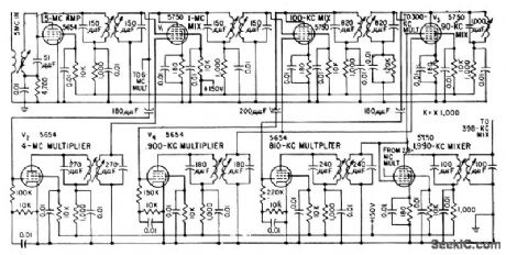
CESIUM_CLOCK_SYNTHESIZER
Published:2009/7/11 1:53:00 Author:May
Crystol 5-Mc oscillator is monitored by natural resonance frequency of cesium (9,192.63184 Mc) to get primary frequency standard. Output signals are 100 kc and 1, 5, 10, and 100 Mc, with accuracy of one port in one billion. Starting with 5 Mc, 9,180 Mc is achieved as harmonic by direct multiplication. Remaining 12.631840 Mc is obtained from 5-Mc source by frequency muhiplication, division, and mixing. Circuit shows input section of synthesizer used for this purpose.-W.A. Mainberger, Primary Frequency Standard Using Resonant Cesium, Electronics, 31:45, p80-85. (View)
View full Circuit Diagram | Comments | Reading(715)
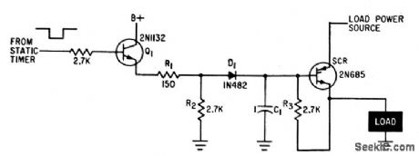
CLOCK_OUTPUT_DRIVER
Published:2009/7/11 1:50:00 Author:May
Driver transistor Q1 is pulsed on at preset time, to supply drive current lo gate of scr so it applies current to load. When scr fires, D1 is back-biased, removing rectifer gate from driver output.-R.S. Reed, Rugged Arming-Fuzing Timer for Atomic Artillery Missile, Electronics,34:38, p48-51. (View)
View full Circuit Diagram | Comments | Reading(616)
NE602_RF_TRANSLATOR_CIRCUIT
Published:2009/7/17 3:09:00 Author:Jessie


This circuit shows how an NE602 is used as an RE translator or mixer in a typical receiver application. Component values depend on operating frequency. (View)
View full Circuit Diagram | Comments | Reading(2712)
10_Hz_CLOCK
Published:2009/7/11 1:50:00 Author:May

Stable and accurate clock is generated by high-precision 100-kHz crystal oscillator and decade divider ehain. Used in 20-meter receiver as part of digital display systemthat shows frequency of received signal aftercounting HFO,LO,and BFO outputs,summing counts, and displaying result.-M. A. Chapman, High Performance 20-Meter Receiver with Digital Frequency Readout, Ham Fladio, Nov 1977, p 56-65. (View)
View full Circuit Diagram | Comments | Reading(1671)
SYNCHRONIZER
Published:2009/7/11 1:48:00 Author:May

For each switch closure, circuit produces one output pulse that is one clock period wide, synchronized with clock. When switch is closed, debouncing latch using 7400 gates goes high and makes flip-flop B high. Next clock pulse makes flip-flop C high and resets flip-flop B. At next clock pulse, flip-flop C goes low to complete cycle of operation.-E. E. Hriv-nak, House Cleaning the Logical Way, 73 Mag-azine, Aug. 1974, p 85-90. (View)
View full Circuit Diagram | Comments | Reading(2676)
Frequency_shift_keyer_using_the_MC1545G_wide_band_amplifier_
Published:2009/7/17 3:09:00 Author:Jessie
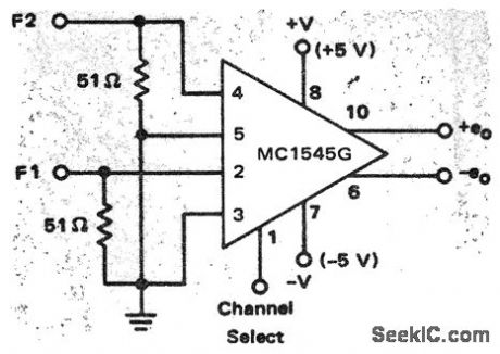
Frequency shift keyer using the MC1545G wide-band amplifier (courtesy Motorola Semiconductor Products Inc.). (View)
View full Circuit Diagram | Comments | Reading(581)
BATTERY_BACKUP_POWER
Published:2009/7/11 1:47:00 Author:May

Provides 60-Hz square-wave output for driving electronic timekeeping circuits from battery during AC power failure, 555 timer is connected as square-wave astable MVBR normally locked to incoming 60-Hz power frequency. Rt should be trimlned for zero beat wiih 60-Hz soulco. When primary power fails, reference voltage disappears and effect of C1 on frequency is minimized. 555 now oscillates at frequency determined by Rt and Ct, Which is 60 Hz. Use 6-V battery.-W. G. Jung, IC Timer Cookbook, Howard W. Sams, Indianapolis, IN, 1977,p 201-203. (View)
View full Circuit Diagram | Comments | Reading(1940)
NARROW_BAND_RADAR_AMPLIFIER
Published:2009/7/17 3:09:00 Author:Jessie
Twin-tee feedback loop tuned to modulating frequency between 60 and 400 cps is used with video crystal and chopper of low-cost c-w radar receiver. Minimum detectable level is -55 dbm.-R. Fleming, Modulation Techniques Cut Radar Cost, Electronics, 35:35, p 56-58. (View)
View full Circuit Diagram | Comments | Reading(1041)
Floating_voltage_controlled_resistor
Published:2009/7/17 3:08:00 Author:Jessie
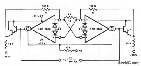
This circuit is similar to that of Fig. 11-6, except that both sections of the XR-13600 (Fig. 11-1B) are used. Each end of the resistor can be at any voltage within the output range of the XR- 13600. EXAR Corporation Databook 1990 p 5-254 (View)
View full Circuit Diagram | Comments | Reading(651)
RF_TRANSISTOR_TESTER
Published:2009/7/11 1:45:00 Author:May

Tells if unknown bipolar or FET transistor is AF, RF, or VHF and whether it is NPN or PNP. Transistor to be tested is placed in frequency-switchable oscillator circuit, and amplitude of oscillation is noted on meter. Highest oscillation frequency corresponds to highest amplification frequency. Six switch positions cover frequency range of 1 to 190 MHz.-F. Brown, An R.F. Transistor Testor, CQ, April 1975, p 35-36 and 66. (View)
View full Circuit Diagram | Comments | Reading(2544)
FSK_with_slope_and_voltage_detection
Published:2009/7/17 3:08:00 Author:Jessie

FSK with slope and voltage detection(courtesy Motorola Semiconductor Products Inc.). (View)
View full Circuit Diagram | Comments | Reading(735)
DIODE_AND_FET_LEAKAGE
Published:2009/7/11 1:44:00 Author:May

FET under test is connected with 22k resistor as source follower, with capacitor C across input from gate to ground. Leakage of FET charges capacitor at rate directly proportional to leakage and inversely proportional to capacitance. With 0.01 μF for C, each volt of change across C indicates stored charge of 10-8 coulomb. This can be interpreted as current in amperes if time for voltage on capacitor to rise 1 V is measured with stopwatch or timer while watching voltmeter. To test diode, connect as shown by dashed line and use good FET in circuit as shown. Article gives design equations; if voltage across C rises 1 V in 38.7 s, leakage current is 0.258 nA.-D. Dilatush, Leakage Testing of Diode and JFETs, EDNMagazine, May 5, 1973, p 72-73. (View)
View full Circuit Diagram | Comments | Reading(844)
MEASURING_TRANSISTOR_REVERSE_VOLTAGE_TRANSFER_RATIO
Published:2009/7/17 3:08:00 Author:Jessie

When output voltage is held constant, 10-my scale of output meter gives direct readings of small-signal value of open-circuit reverse-voltage transfer ratio h-rb over range of 0.0001 to 0.001.-Texas Instruments Inc., Transistor Circuit Design, McGraw-Hill, N.Y., 1963, p 72. (View)
View full Circuit Diagram | Comments | Reading(1001)
| Pages:786/2234 At 20781782783784785786787788789790791792793794795796797798799800Under 20 |
Circuit Categories
power supply circuit
Amplifier Circuit
Basic Circuit
LED and Light Circuit
Sensor Circuit
Signal Processing
Electrical Equipment Circuit
Control Circuit
Remote Control Circuit
A/D-D/A Converter Circuit
Audio Circuit
Measuring and Test Circuit
Communication Circuit
Computer-Related Circuit
555 Circuit
Automotive Circuit
Repairing Circuit