
Circuit Diagram
Index 785
R_C_RECEIVER_PREAMPLIFIER
Published:2009/7/17 3:18:00 Author:Jessie
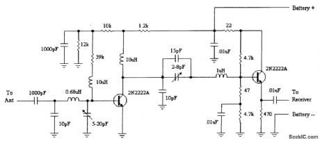
The circuit shown is small, draws little current, and is easily fabricated on a perfboard-just keep the wires short and the bypass capacitors close to their position on the schematic. To install, make a break in the wire from the antenna and insert the preamplifier. With proper trimming, this circuit yields about 20 dB of gain. (View)
View full Circuit Diagram | Comments | Reading(619)
Phase_sensitive_detector_with_square_wave_reference
Published:2009/7/17 3:18:00 Author:Jessie

Phase-sensitive detector with square-wave reference. If the input and reference are in phase the output is positive. If they are 180° out of phase the output is negative (courtesy Analog Devices, Inc.). (View)
View full Circuit Diagram | Comments | Reading(2828)
Triangular_square___wave_VCO
Published:2009/7/17 3:17:00 Author:Jessie

This classic triangular/square-wave generator (chapter 5) uses both sections of an XR-13600 (Fig. 11-1B). With the values shown, the oscillator provides signals from 200 kHz to below 2 Hz when IC is varied from 1 mA to 10 nA.The output amplitudes are set by IA×RA. Notice that the peak differential-input voltage must be less than 5 V to prevent zenering the inputs. EXAP Corporahon Databook 1990 p 5-255 (View)
View full Circuit Diagram | Comments | Reading(821)
AUDIO_MIXER
Published:2009/7/17 3:17:00 Author:Jessie

An audio mixer is a handy circuit that will combine two or more audio signal sources into one signal channel. The figure shows an audio mixer that is built around the LM3900 CDA. The crux of this circuit is the three input networks, principally R3, R4, and R5. These resistors are connected to different input sources (labeled VIN1,VIN2, and VIN3). Those three resistors all connect to the inverting input of the CDA. The gain is approximately
AV=R2/Rxwhere Rx is the value of any one input resistor. The output voltage is
Vo=R2[(VIN1/R3)+(VIN2/R4)+(VIN3/R5)If resistor R2 is made variable, then the potentiometer used for R2 will serve as a master gain control for the audio mixer. (View)
View full Circuit Diagram | Comments | Reading(7238)
Digitally_programmable_limit_detector
Published:2009/7/17 3:16:00 Author:Jessie

Digitally programmable limit detector(courtesy Analog Devices,Inc.). (View)
View full Circuit Diagram | Comments | Reading(583)
pH_METER
Published:2009/7/17 3:16:00 Author:Jessie

Beckman model W industrial-type pH meter is d-c amplifier designed for measuring potentials generated by pH-sensitive electrodes. Output will drive most recorders.R32 is used only with 4 to 14 pH meter, and R33 only with -1 to 9 pH meter.-G. C. Car. roll, Industrial Instrument Servicing Handbook, McGraw-Hill, N.Y., 1960, p 7-4. (View)
View full Circuit Diagram | Comments | Reading(2021)
VARIABLE_RESISTOR_CONTROLLED_REGENERATIVE_RECEIVER
Published:2009/7/17 3:16:00 Author:Jessie

View full Circuit Diagram | Comments | Reading(620)
Voltage_controlled_state_variable_filter
Published:2009/7/17 3:15:00 Author:Jessie

This circuit uses both sections of an XR-13600 (Fig. 11-1B) to form a state-variable filter (with both low-pass and bandpass outputs). EXAR corporation Databook, 1990 p,5-255 (View)
View full Circuit Diagram | Comments | Reading(865)
Missing_pulse_detector_using_an_ECG955M_timer_oscillator_chip
Published:2009/7/17 3:15:00 Author:Jessie

Missing pulse detector using an ECG955M timer/oscillator chip. The timing cycle is continuously reset by the input pulse train. A change in frequency or missing pulse allows completion of the timing cycle, which causes a change in the output level. The time delay should be set a little longer than normal between pulse for this reason (courtesy GTE Sylvania Incorporated). (View)
View full Circuit Diagram | Comments | Reading(860)
SCA_RECEIVER
Published:2009/7/17 3:15:00 Author:Jessie
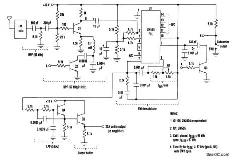
A simple PLL-based FM demodulator can be made to demodulate two subcarriers and provide a source of background music. The input to this receiver is fed from the wideband audio output from an FM radio's first FM detector. This is the point that feeds the FM stereo demodulator in an FM receiver. Care should be taken to ensure that the signal is tapped off at a point which hasn't yet been filtered [the subcarrier(s) are still present]. This FM input signal is then passed through a second-order high-pass filter and peaker stage (Q1), which serves to bandpass and provide additional gain within the input spectrum prior to the FM demodulator input. The FM detection is accomplished by a simple LM565 PLL IC (U1) operating as an FM demodulator. The PLL's VCO is tuned to 91 kHz via RT/CT. The demodulated output signal is available at pin 7, which is followed by a second-order LPF/buffer combination (Q4). The characteristics of this filter can be modified to suit the user. The design shown has an audio corner frequency of about 5 kHz. The filtered output is the recovered audio output and is the input to an audio amplifier. To choose the second subcarrier (67 kHz), the peaker and VCO are gang-tuned by the Q2 and Q3 saturating switch transistors. These devices switch in appropriate-valued parallel capacitors to retune the peaker and VCO to the proper frequency for reception of the second subcarrier signal. Circuit values shown are for an FM level of about 50 to 300 mV rms at the input to the peaker stage. In addition, the PLL dynamic characteristics can be altered as desired by modifying the loop filter. The typical recovered audio level at pin 7 of U1 is 200 mV rms. To receive SCA signals, the FM receiver can simply be tuned to normal FM stations, and then the presence of either or both subcarriers can be checked. (View)
View full Circuit Diagram | Comments | Reading(5220)
Frequency_shift_keyer_tone_generator_using_two_8_pin_DIPs_and_one_transistor
Published:2009/7/17 3:14:00 Author:Jessie

Frequency-shift keyer tone generator using two 8-pin DIPs and one transistor (courtesy GTE Sylvania Incorporated). (View)
View full Circuit Diagram | Comments | Reading(812)
TRANSISTORIZED_CHRONOTRON_MEASURES_COAX_DELAY
Published:2009/7/17 3:13:00 Author:Jessie

Start switch triggers avalanche transistor Q1, generating millimicrosec pulse that travels down unknown cable and returns to trigger new pulse. Digital counter is used to mesaure prr, which is proportional to cable delay. Q2 shapes counter pulse.-E. F. Laine, Getting Subnano-second Precision in Coax Cable Delay Measurements, Electronics, 36:5, p 39-41. (View)
View full Circuit Diagram | Comments | Reading(1153)
Self_generating_FSK_
Published:2009/7/17 3:13:00 Author:Jessie

Self-generating FSK (courtesy Motorola Semiconductor Products Inc.). (View)
View full Circuit Diagram | Comments | Reading(585)
Voltage_controlled_Butterworth_filter
Published:2009/7/17 3:12:00 Author:Jessie

This circuit uses both sections of an XR-13600 (Fig. 11-1B) to form a 2-pole Butterworth low-pass filter. EXAH Corporatton Databook 1990, p 5-254 (View)
View full Circuit Diagram | Comments | Reading(596)
MICROMICROAMMETER
Published:2009/7/17 3:12:00 Author:Jessie

Uses vibrating capacitor, electrometer amplifier, and electronic servo in which amplifier attempts to maintain input at ground potential regardless of magnitude of voltage developed across input resistor by very small signal current being measured.-G. C. Carroll, Industrial Instrument Servicing Handbook, McGraw-Hill, N.Y., 1960, p 6-6. (View)
View full Circuit Diagram | Comments | Reading(798)
FOUR_PHASE_CLOCK
Published:2009/7/11 2:00:00 Author:May

Provides expandable 3-bit binary output and four overlapping clock pulses for each unique binary output. A-output of 7493 binary counter is used along with dock input to form four-phase overlapping clock function. Article indudes timing diagram that shows sequence of output pulses. Developed for use in addlessing multiplexers, ROMs, and other digital units,-B. Brandstedt, Clock Pulse Generator Has Addressable Output, EDN Magazine. Dec. 15, 1972, p 42. (View)
View full Circuit Diagram | Comments | Reading(1695)
Voltage_controlled_high_pass_filter
Published:2009/7/17 3:12:00 Author:Jessie

This circuit is similar to that of Fig. 11-9, except that the single RC rolloff is below the defined cutoff frequency. EXAR corpora,ion Databook, 1990 p 5-254 (View)
View full Circuit Diagram | Comments | Reading(587)
TWO_IC_MEDIUM_WAVE_RECEIVER
Published:2009/7/17 3:12:00 Author:Jessie
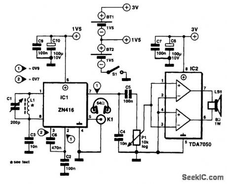
The antenna is an inductor, L1, consisting of about 60 turns of 0.2-mm (SWG36) enameled copper wire on a ferrite rod with a diameter of 12 mm and a length of about 12 cm. The inductor is tuned with a 500-pF foil-dielectric variable capacitor, C1. The audio power amplifier, a TDA7050, is required only if you want to use a small loudspeaker instead of, or in addition to, the headphones. The AF power amplifier also adds the luxury of a volume control to the receiver. The receiver IC operates at 1.54 V from only one of two series-connected AA (penlight) batteries, which supply 3 V to the TDA7050. Current consumption is of the order of 8 mA. (View)
View full Circuit Diagram | Comments | Reading(1122)
CLOCK_FOR_REGULATED_SUPPLY
Published:2009/7/11 2:00:00 Author:May

Single RCA CD4009A serves as clock generator and mono for driving regulated power supply having fold-back current-limiting protection. Rtc and Ctc are maior frequency-determining components. RS should be made equal to or greater than 2Rtc, Article gives equation for period T of oscillator, which ranges from about 2.2 to 2.5 times Rtc Ctc.-J. L. Bohan, Clocking Scheme Improves Power Supply Short-Circuit Protection, EDN Magazine, March 5, 1974, p 49-52. (View)
View full Circuit Diagram | Comments | Reading(569)
5_W_80_m_CW_TRANSCEIVER
Published:2009/7/11 1:58:00 Author:May

This transceiver has a 3-stage transmitter and a direct-conversion receiver. Q1 is the transmitter's oscillator, and the frequency is controlled by X1, which also serves as the receiver local oscillator. Buffer Q2 drives final amplifier Q3 to about 5 W output. The B+ lead to these stages is keyed. The receiver consists of mixer Q4 followed by high gain amplifiers Q5/Q6/Q7. The audio signal appears at the secondary of Q7. In the transmit mode, Q5/Q6/Q7 serve as a sidetone oscillator. A 6PDT switch is required for the T/R switching. (View)
View full Circuit Diagram | Comments | Reading(1588)
| Pages:785/2234 At 20781782783784785786787788789790791792793794795796797798799800Under 20 |
Circuit Categories
power supply circuit
Amplifier Circuit
Basic Circuit
LED and Light Circuit
Sensor Circuit
Signal Processing
Electrical Equipment Circuit
Control Circuit
Remote Control Circuit
A/D-D/A Converter Circuit
Audio Circuit
Measuring and Test Circuit
Communication Circuit
Computer-Related Circuit
555 Circuit
Automotive Circuit
Repairing Circuit