
Circuit Diagram
Index 793
TRANSISTOR_DIODE_TESTER
Published:2009/7/10 23:49:00 Author:May

Checks for polarity, shorts, and opens in one measurement, using six LEDs as indicators. Circuit derives three-phasewaveform from 2-kHz ring-of-three oscillator for application to device under test through LEDs. Oscillator waveform serves to make each pair of device terminals forward, reverse, and unbiased in turn for one-third of a cycle. Current flowing into device turns on red LED, and current flowing out turns on green LED, to indicate polarity and position of base lead.-N. E. Thomas, Semiconductor Tester, Wireless World, March 1977, p 43. (View)
View full Circuit Diagram | Comments | Reading(2224)
ADC_CONVERTER_SYNCHRONOUS_DEMODULATION
Published:2009/7/17 3:52:00 Author:Jessie

Digital radio techniques promise to dramatically enhance receiver capabilities. Directly converting the IF (intermediate frequency) to a digital signal facilitates digital signal processing of demodulated signals. The example described here features an AM radio detector circuit for the typical IF of 455 kHz. For RF demodulation, the input is sampled at a rate exactly equal to the input-signal frequency. The digital output signal, which is actually an alias of the input, is the recovered modulation. (View)
View full Circuit Diagram | Comments | Reading(2221)
CRYSTAL_CONTROLLED_TIMER
Published:2009/7/10 23:48:00 Author:May

Intersil 7209 clystal oscillator provides buffered CMOS output capable of driving over five TTL loads any crystal frequency up to 10 MHz.Used in applications requiring high-accuracy buffered timingsignals for system clocks.-B.O.'Neil,IC Timers-the Old Reliable 555 Has Company,EDN Magazine, Sept.5,1977,p 89-93. (View)
View full Circuit Diagram | Comments | Reading(643)
MOS_FOUR_GATE_CLOCK
Published:2009/7/10 23:47:00 Author:May

Only one 4001 CMOS quad two-input NOR-gate 10 is needed for symmetrical complementary-output clock having good temperature and supply stability.Gates U1 and U2 form astable oscillator producing positive-going pulses used to triggir divide-by-2 flip-flop U3-U4. Circuit will operate over wide range of supply voltages and temperatures,-M,Eaton,Symmetrical CMOS clock is Inexpensive,EDN Magazine.March 20,1974,p 80 and 83. (View)
View full Circuit Diagram | Comments | Reading(575)
5_V_AT_3_A
Published:2009/7/17 3:52:00 Author:Jessie

National LM5000 voltage regulator having built-in overload protection is basis of small bench supply for TTL work. Filament transformer rated 12.6 V at 3 A feeds full-wave bridge rectifier rated 200 PIV at 6 A, such as Radio Shack 276-1172. U1 requires heatsink insulated from chassis. Output filter C3 should be mounted directly on regulator terminals to minimize circuit oscillation. Output should read within 100 mV of 5 V. Radio Shack 276-047 LED serves as output indicator. Use 0.22-μF bypass between pins 2 and 3 of U1.-K. Powell, The 5 x 3 Power Supply, QST, May 1977, p 25-26. (View)
View full Circuit Diagram | Comments | Reading(552)
RC_CLOCK
Published:2009/7/10 23:46:00 Author:May

Simple TTL clock generator is suitable for most TTL systems. Requires only half of hex inverter package and three passive com ponents. Clock frequency depends on value of C: 200 pF gives 5 MHz; 1600 pF gives 1 MHz; 0.018 μF gives 100 kHz; and 0 18 μF gives 10 kHz.-Circuits, 73 Magazine, Aug. 1974, p 99. (View)
View full Circuit Diagram | Comments | Reading(2733)
3_wire_plus_digital_ground_data_transfer_system_
Published:2009/7/17 3:52:00 Author:Jessie

3-wire plus digital ground data transfer system (courtesy Analog Devices, Inc.). (View)
View full Circuit Diagram | Comments | Reading(559)
ADUSTABLE_CLOCK_FOR_MPU
Published:2009/7/10 23:46:00 Author:May

Two MC8602 cross-coupled mono MVBRs with individual pulse-width adjustments are used as clock oscillator to provide frequency flexibility for exnentation with data throughput,real-time operation with interrupts,and diagnosis of systiming problems,Required nonoverlapping clock pulses for phases 1 and 2 are generated by proagation delays through MVBRs,Transistors used for drivers are MPQ6842.- Microessor Applications Manual (Muturola Series in Solid-State Electronics), McGraw-Hill, New, York, NY, 1975, p 4-5—4-10. (View)
View full Circuit Diagram | Comments | Reading(583)
Two_wire_differential_data_transmission_system_using_an_MC75110_driver_and_an_MC75107_receiver
Published:2009/7/17 3:51:00 Author:Jessie

Two-wire differential data transmission system using an MC75110 driver and an MC75107 receiver (courtesy Motorola Semiconductor Products Inc.). (View)
View full Circuit Diagram | Comments | Reading(553)
FET_AMPLIFIER_WITH_MECHANICAL_CHOPPER
Published:2009/7/10 23:44:00 Author:May

Gives readings down to10 nanovolls,with wideband response, because of remarkably low noise performance. Chopper frequency can be up to 1,500 cps.-Airpax Electronics (ad), Electronics, 39:15, p170. (View)
View full Circuit Diagram | Comments | Reading(1463)
13_V_AT_2_A_WITH_PNP_TRANSISTORS
Published:2009/7/17 3:50:00 Author:Jessie

Reference voltage source q1 is 2N301, while series-pass regulator Q2 is 2N1523 D5 is 1N5245 15-V zener Secondary of T1 is 16-19 V, or can be 6-V and 12-V filament transformers in series. Article tells how to adapt circuit for other output voltages. - R. B. Joerger, Power Supply, 73 Magazine, Holiday issue 1976, p 40-41. (View)
View full Circuit Diagram | Comments | Reading(1042)
AM_MODULATOR_LIMITING_AMPLIFIER
Published:2009/7/17 3:50:00 Author:Jessie
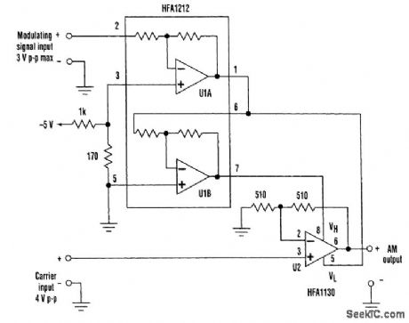
Limiting amplifiers also can be put to work in AM modulators. The fast overdrive recovery time and wide bandwidth of the clamp inputs allows these inputs to be driven by high-frequency ac, can as well as dc signals. When driven at the appropriate levels, the clamp inputs can be used to form an amplitude modulator. The HFA1130 limiting amplifier is driven by a 4-V p-p carrier signal. The gain of 2 through the HFA1130 ensures that the carrier amplitude is sufficient to drive the output over its±3.3-V range. The HFA1212 performs the necessary level shifting and inversion to convert the modulating signal input into a pair of antiphase signals that control the high and low clamp inputs. U1A inverts the signal and level-shifts to -1.5 V. U1B inverts that signal, forming a complementary signal centered at + 1.5 V. With a signal input of 0 V, U2 produces a 3-V p-p output at the carrier frequency. As the signal input varies, U2 produces a symmetrically modulated carrier with a maximum ampli-tude of6 V p-p. The 2300-V/μs slew rate of the HFA1130 limits 6-V p-p amplitude carrier signals to a frequency of 61 MHz. If adjusted for lower output-signal levels, the carrier and modulating frequencies can be increased to well above 100 MHz. (View)
View full Circuit Diagram | Comments | Reading(1604)
GATE_TURNOFF_D_C_CHOPPER
Published:2009/7/10 23:41:00 Author:May

Will chop 1 kw at 1 kc. Ralio of on time to off time can be adjusted to control power, voltage, tem-perature, and other parameters. Shunt circuit allows larger currents to be chopped.-J. W.Motto, Jr, Switching Circuits Using the Gote Turnoff Controlled Rectifier, EEE, 11:3, p52-55. (View)
View full Circuit Diagram | Comments | Reading(534)
Dual_Schmitt_trigger_used_as_a_2_wire_differential_line_receiver_
Published:2009/7/17 3:50:00 Author:Jessie

Dual Schmitt trigger used as a 2-wire differential line receiver (courtesy Motorola Semiconductor Products Inc.). (View)
View full Circuit Diagram | Comments | Reading(785)
JFET_CURVE_TRACER
Published:2009/7/10 23:37:00 Author:May

Quad opamp and J176 JFET switch form basis of simple curve tracer that can be used with any CR0. Circuit displays drain current versus gate voltage for both Pchannel and N-channel JFETs at constant drain voltage. Sweep time is 10 ms. Sweep rate is 0.5 V/mswith maximum gate voltage of ±5V. Drain current is fed to vertical input and gate voltage to horizontal input.- FET Databook, National Semiconductor, Santa Clara, CA, 1977, p 6-506-51. (View)
View full Circuit Diagram | Comments | Reading(1030)
True_rms_converter
Published:2009/7/17 3:49:00 Author:Jessie

This circuit uses both sections of an XR-13600 (Fig. 11-1B). The circuit is essentially an AGC amplifier, which adjusts the gain such that the output of A1 is constant. The calibration potentiometer is set such that VO reads directly in rms volts. EXAR Corporation Databook 1990, p 5-257 (View)
View full Circuit Diagram | Comments | Reading(1069)
HALL_GENERATOR_CHOPPER_AMPLIFIER
Published:2009/7/10 23:36:00 Author:May

D-c signal voltage to be chopped is applied as control current of Hall generator. Magnetic field for generator is pulsed at 60 cps by driver circuit. Output is pulsating d-c voltage that is product of the two inputs. Error in input d-c versus output a-c is 2.5% for tem-perature range of -20 to 50℃. Can be used as d-c, a-c, or r-f microammeler.-T. J. Marcus, Highly Sensitive Electronic Chopper, Electronics, 32:40, p67-68. (View)
View full Circuit Diagram | Comments | Reading(592)
AF_SIGNAL_INJECTOR
Published:2009/7/10 23:36:00 Author:May

Can be built into penlight housing, using single penlight cell or 1.5-V mercury cell for power. Output probe for feeding signal to audio circuit under test is about linch length of stiff wire, pointed. For more output, run ground lead to equipment under test.Q1 can be HEP253, 2N519, 2N741A, 2N2929, or equivalent. Q2 can be HEP3, 2N1280, 2N2273, SK3005, or equivalent. Adjust R, and R, for good output, and ad just R3 as required for good tone.To use, touch probe to input of any receiver or high-fidelity audio circuit. Tone should be heard from loudspeaker if circuit is good between probe and loudspeaken-C.J. Schauers, Transistorized Signal Tracer, CQ4 Sept. 1973, p 12 and14. (View)
View full Circuit Diagram | Comments | Reading(941)
60_hertz_nicad_battery_charger_with_voltage_sensing
Published:2009/7/17 3:49:00 Author:Jessie

60-hertz nicad battery charger with voltage sensing. Hex inverter is an MC789P (courtesy Motorola Semiconductor Products Inc.). (View)
View full Circuit Diagram | Comments | Reading(934)
SIMPLE_RING_DETECTOR
Published:2009/7/10 23:33:00 Author:May

This circuit detects the 20-Hz approximately 86-Vrms ring signal on telephone lines and initiates action in an electrically isolated circuit. Typical applications include automatic answering equipment, interconnect/interface and key systems. The detector is the simplest and provides about a 1-mA signal for a 7-mA line, which loads for 0.1 s after the start of the ring signal. The time-delay capacitor provides a degree of dial-tap and click suppression, and filters out the zero crossing of the 20-Hz wave. (View)
View full Circuit Diagram | Comments | Reading(1182)
| Pages:793/2234 At 20781782783784785786787788789790791792793794795796797798799800Under 20 |
Circuit Categories
power supply circuit
Amplifier Circuit
Basic Circuit
LED and Light Circuit
Sensor Circuit
Signal Processing
Electrical Equipment Circuit
Control Circuit
Remote Control Circuit
A/D-D/A Converter Circuit
Audio Circuit
Measuring and Test Circuit
Communication Circuit
Computer-Related Circuit
555 Circuit
Automotive Circuit
Repairing Circuit