
Circuit Diagram
Index 790
APPLIANCE_CUTOFF_TIMER
Published:2009/7/11 0:58:00 Author:May

Suitable for cutting off an appliance or other ac load, this timer will cut the ac power after a period determined by R1/C3, as shown, for about 40 minutes. K1 is a relay that should handle about 10 A. S1A and S1B is a momentary switch that starts the timer cycle. (View)
View full Circuit Diagram | Comments | Reading(937)
SCR_gas_smoke_detector_with_half_wave_control_of_24_volt_AC_horn
Published:2009/7/17 4:02:00 Author:Jessie

SCR gas/smoke detector with half-wave control of 24-volt AC horn. The Taguchi gas sensor (TGS) consists of an N-type semiconductor of tin dioxide encased in a noble metal wire heater, which also serves as an electrode (courtesy Motorola Semiconductor Products Inc.). (View)
View full Circuit Diagram | Comments | Reading(1461)
PROGRAMMABLE_TIMER_FOR_LONG_INTERVALS
Published:2009/7/11 0:56:00 Author:May


By using an RC oscillator and a programmable divider, this counter can run for hours. An interval oscillator runs at a frequency given by (see figure schematic):By using, for example, R4 = 390 kΩ and C2 = 10 μF and Rz, the oscillator can run at 0.1 Hz. Divided by 65536, this is a cycle of approximately 655 000 s (182 hours, slightly more than a week). (View)
View full Circuit Diagram | Comments | Reading(1584)
Norton_inverting_ac_amplifier
Published:2009/7/17 4:02:00 Author:Jessie
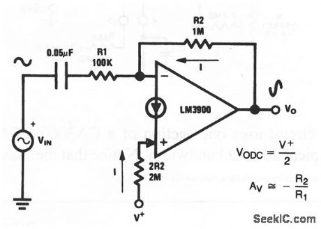
This circuit uses one section of an LM3900 to form an inverting ac amplifier with single-supply biasing (the circuit is biased from the same supply used to operate the amplifier). Figure 11-32B shows the pin connections for all four sections of an LM3900. If ripple voltages are present on the V+ power-supply line, the voltages will appear at the output with a gain of one-half. To eliminate this problem, one source of ripple-filtered voltage can be provided, and then used for many amplifiers, as shown in Fig. 11-33. National Semiconductor Linear Applications Handbook, 1991 p 218 220. (View)
View full Circuit Diagram | Comments | Reading(923)
LONG_INTERVAL_PROGRAMMABLE_TIMER
Published:2009/7/11 0:53:00 Author:May

Using an RC oscillator, an up to 24-stage ripple counter (÷) 16777216 or 224, and a 0.1-Hz count-rate with R=39 kΩ, C2 =0.001 μF, and R4-220 k0 for example, the count cycle would take about 654 s. This example shows the capabilities of this time circuit, using the Motorola MC14536 timer. A low-frequency oscillator can be used for longer time periods. (View)
View full Circuit Diagram | Comments | Reading(1571)
AC_OPERATED_WATERING_CONTROL_SYSTEM
Published:2009/7/17 4:02:00 Author:Jessie

Ac operation of the circuit reduces possible electrolysis effects over time. Two probes are inserted into the soil. When the soil is wet, it is more conductive and Q1 conducts, cutting Q2 off. As the soil dries, Q1 loses bias, allowing Q2 to turn on, actuating the relay (RY1). RY1 closes, operating the watering-system control valve. When the soil is sufficiently moist, Q1 turns on, cutting off Q2, RY1, and the water valve. R2 sets the trip level. (View)
View full Circuit Diagram | Comments | Reading(739)
1_min_RECORD_PLAYBACK_CIRCUIT
Published:2009/7/17 4:02:00 Author:Jessie

You can cascade several ISD1020As to increase a system's capacity. A circuit to create a 1-minute message is shown. With this conftguration, a message is stored across chip boundaries in a manner transparent to the user. Changing from Record to Play resets the MSP to the beginning of the first message in the series. The next Play proceeds under control of CB. The circuit operates exactly like that for a single device. (View)
View full Circuit Diagram | Comments | Reading(728)
Ionization_chamber_smoke_detector_using_discrete_transistors_for_alarm_oscillators
Published:2009/7/17 4:01:00 Author:Jessie

Ionization-chamber smoke detector using discrete transistors for alarm oscillators(Courtesy Motorola Semiconductor Products Inc.). (View)
View full Circuit Diagram | Comments | Reading(1202)
TAPELESS_PLAY_ONLY_DEVICE
Published:2009/7/17 4:01:00 Author:Jessie

This requires a prerecorded message to be preprogrammed in the ISD1020A. To play a message, set the switch to the +5-V position. The ISD1020A plays the entire contents one time, then stops.Because CB is tied low, the set end-of-message bits are ignored. Momentarily changing the switch to open, then back to +5 V makes the ISD1020A play again. (View)
View full Circuit Diagram | Comments | Reading(923)
Tri_level_comparator
Published:2009/7/17 4:01:00 Author:Jessie

This circuit uses all three sections of a CA3060 to form a tri-level comparator, which has three adjustable limits. If either the upper or lower limit is exceeded, the appropriate output is activated until the input signal returns to a selected intermediate value. Such comparators are used in industrial control applications. The lower and upper limits are set by R 1 and R2, respectively. R3 and R4 set the intermediate limit. When both R3 and R4 are the same value, the intermediate limit is midway between the upper and lower limits. The loads shown are 5-V 25-mA lamps. Harris Semiconductor Linear & Telecom ICs 1991 p 3-51 (View)
View full Circuit Diagram | Comments | Reading(2453)
RAIN_SENSOR
Published:2009/7/17 4:00:00 Author:Jessie
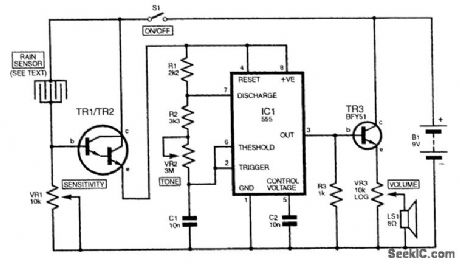
The figure shows a simple rain sensor design that incorporates pitch and volume controls in the alarm signal. Whenever the sensor is bridged by droplets of water, the Darlington transistor TR1/TR2 will conduct. This enables IC1, a 555 astable tone generator, to function, powering a small loud-speaker through a driver transistor (TR3). VR2 determines the pitch of the audio tone, which can be anything from about 25 Hz to 18 kHz, while VR3 adjusts the volume. The sensitivity of the circuit is set by VR1. The Darlington pair could be constructed with two separate ZTX300s or a single TlP122. For the sensor, use a small piece of stripboard, linking alternate strips into an interlocking design. The circuit will operate from a standard 9-V PP3-type battery. (View)
View full Circuit Diagram | Comments | Reading(3762)
TAPELESS_RECORD_PLAY_DEVICE
Published:2009/7/17 4:00:00 Author:Jessie

The schematic for a record/play device with an audio power amplifier added is shown.
●A four-section DIP switch is used to activate the Chip enable, Power down, Playback, and Record functions.●An LED detects an end-of-message condition. It remains off during Record or Play and turns on when a message ends.●A three-terminal electret microphone is used for recording.●The only off-board components are the microphone, speaker, and power supply. For optimum sound, the speaker should be baffled (placed in an enclosure). Four 1.5-V AA cells can be used as a power source. (View)
View full Circuit Diagram | Comments | Reading(1474)
TRANSMIT_TIME_LIMITER
Published:2009/7/11 0:51:00 Author:May

This circuit prevents making transmissions that are too long, which time out repeaters and/or tie up a communications channel too long. On transmit, the PTT (push to talk |ipe) from the microphone is at ground. This causes one input of the AND gate (4081) to go high. The 555 is held in the reset mode. An MC1453B monostable multivibrator generates a pulse to the 555 and causes it to produce a gate of length approximately 1.1RC, where R is selected for desired time delay and C is 100 μF. The output of pin 3 of the 555 causes the 4081 gate to go high, turns on Q1, and keys the transmitter. At the end of the cycle (1.1RC), the AND gate will lose one input, which turns off Q1 and unkeys the transmitter. (View)
View full Circuit Diagram | Comments | Reading(928)
MAINS_POWERED_TIMER
Published:2009/7/11 0:48:00 Author:May

This timer can be inserted in a power line to provide a controllable delay before a load is energized. The mains voltage is reduced'by C3 and rectified to give about 30 V across C1. This potential charges C2 slowly via R4/P1. When UC2 reaches about 14 V, electronic switch T1/T2 actuates a solid-state relay (a Sharp S202DS). When the mains voltage is removed, C2 discharges rapidly via D6 and R10. The delay extends from 15 s (P1 set to minimum resistance) to 5 min (P1 set to maximum resistance).The solid-state relay needs cooling in accordance with the current drawn by the load: at up to 1 A, no heatsink is required; at 1 to 3 A (max), a 5 x 5 cm heatsink is advisable.During the building of the circuit, consideration must be given to safety because many parts will be at mains potential. For instance, fitting the unit in an ABS or other man-made fiber enclosure is a must. If a potentiometer is used for P1, its spindle should be insulated. If a preset is used, it must not be accessible through a hole in the enclosure.Switch S1 is a DPST that disconnects the circuit from the mains. Nevertheless, the only way to safely work on the circuit is to unplug the mains socket and allow C3 sufficient discharge time. (View)
View full Circuit Diagram | Comments | Reading(874)
20_dB_amplifier
Published:2009/7/17 4:00:00 Author:Jessie
This circuit uses one section of a CA3060 OTA to form a 20-dB amplifier with a typical 20-kHz bandwidth.Notice that the bias input is connected to a fixed+6V. (View)
View full Circuit Diagram | Comments | Reading(878)
HIGH_ACCURACY_THERMOMETER
Published:2009/7/11 0:46:00 Author:May

This circuit combines a current source and a platinum RTD bridge to form a complete high-accuracy thermometer. The ground,referred RTD sits in a bridge that is composed of the current drive and the LT1009 biased resistor string. The current drive allows the voltage across the RTD to vary directly with its temperature-induced resistance shift. The difference between this potential and that of the opposing bridge leg forms the bridge output. The RTD's constant drive forces the voltage across it to vary with its resistance, which has a nearly linear positive temperature coefficient. The nonlinearity could cause several degrees of error over the circuit's 0℃ -400℃ operating range.The bridge's output is fed to instrumentation amplifier A3, which provides differential gain, while simultaneously supplying nonlinearity correction. The correction is implemented by feeding a portion of A3's output back to A1's input via the 10- to 250-kΩ divider. This causes the current supplied to Rp to slightly shift with its operating point, compensating sensor nonlinearity to within ±0.05℃. A1B, provid-ing additional scaled gain, furnishes the circuit output.To calibrate this circuit, follow the procedure given in the diagram. (View)
View full Circuit Diagram | Comments | Reading(934)
SINGLE_dc_SUPPLY_THERMOMETER
Published:2009/7/11 0:41:00 Author:May

Using a J-type thermocouple, this circuit can indicate temperatures from -350° to 400° with a 6-V supply or -50 to + 100° with a 3-V lithium battery. The AD954 produces 10 mV/°C output to the MAX 138 digital voltmeter chip, which drives the LCD display. (View)
View full Circuit Diagram | Comments | Reading(1350)
ELECTRONIC_THERMOMETER
Published:2009/7/11 0:39:00 Author:May

This thermometer uses an NTC thermistor (R10) to produce a dc voltage that decreases with tem-perature, to drive an IC that lights one of the 16 LEDs as a function of this voltage. R11 is a light-depen-dent resistor that adjusts the LED brightness as a function of ambient light. (View)
View full Circuit Diagram | Comments | Reading(0)
FAULT_TOLERANT_RELAY_DRIVER
Published:2009/7/17 4:09:00 Author:Jessie

Mechanical relays are useful in remote-switching applications that require electrical isolation between control and switched circuits. The traditional approach for driving the relay coils uses a single-transistor common-emitter switch. The figure shows a circuit that can reduce the likelihood of having an unrecoverable failure in the relay driver circuit. Additional transistor switches, inserted in series with the original controlling transistors, maintain proper operation if a single transistor fails. The diodes connected to the upper transistors prevent reverse base-current flow if the collector-base junctions break down. The diodes connected to the lower transistor provide proper biasing for the circuit. The upper and lower transistors will have a similar Vbe because they are the same type and have nearly identical currents. Therefore, the Vbe of the lower transistor will be about the same as one diode voltage drop, and the device will be operating in the active region. Power to the relays can be provided by one of two voltage sources connected together through 'diodes in a wired-OR configuration. The additional diode clamps the coil inductance voltage spike in the event that one of the suppression diodes fails shorted. (View)
View full Circuit Diagram | Comments | Reading(2464)
INEXPENSIVE_LINERA_THERMOMETER
Published:2009/7/11 0:39:00 Author:May


As a sensor in the design of this linear thermometer, the LM34 is used. The output is the difference between two base-emitter voltages vEB of two transistors operated at different collector-current densi-ties. The voltage difference (△VEB) is:where the current densities are IC1 and IC2,k is Boltzrnann's constant, and q is the electron charge. Because all factors, including the ratio IC1/IC2 are constant, the output of the LM34 (Nationgl Semiconduc-tor) is a linear function of T in the range over -50°to 300°F, which provides the output voltage of 10 mV/ °F with a max. nonlinearity of ±0.35°F.The output of the LM34 is amplified by a three-op-amp instrumentation amplifier. The fourth op amp gives the possibility to control the offset voltage of the amplifier. The gain A of the instrumentation amplifier can be set to any desired value by the choice of the resistance R2 only. (View)
View full Circuit Diagram | Comments | Reading(707)
| Pages:790/2234 At 20781782783784785786787788789790791792793794795796797798799800Under 20 |
Circuit Categories
power supply circuit
Amplifier Circuit
Basic Circuit
LED and Light Circuit
Sensor Circuit
Signal Processing
Electrical Equipment Circuit
Control Circuit
Remote Control Circuit
A/D-D/A Converter Circuit
Audio Circuit
Measuring and Test Circuit
Communication Circuit
Computer-Related Circuit
555 Circuit
Automotive Circuit
Repairing Circuit