
Circuit Diagram
Index 795
EDGE_DETECTOR
Published:2009/7/10 23:22:00 Author:May

Half of 9014 quad EXCLUSIVE-OR gate serves for generating output pulse for both low-to-high and high-to-low transitions of input signal. Used for regenerating clock in self-clocking pulse-width modulation transmission system, Circuit acts as frequency doublerfor square-wave input. With 1000 pF for C, output pulse width is 70 ns; for 200 pF, width is 30 ns; and when C is 0, width is 10 ns.-Circuits, 73 Magazine, Aug. 1974, p 99. (View)
View full Circuit Diagram | Comments | Reading(0)
OP_AMP_VLF_RECEIVER
Published:2009/7/17 3:42:00 Author:Jessie

The figure shows the circuit diagram for an operational-amplifier VLF receiver. The circuit in the figure uses a virtual-inductor front end. A virtual inductor is a circuit that acts like an inductor, but isn't. Operational amplifiers AIA and AIB form a gyrator circuit. The inductance of this circuit is the product of the components shown between A1A and A1B [C3× 3300 × (R2 \+ R3)]. Capacitor C2 resonates with the virtual inductance produced by the gyrator circuit to tune the desired frequency. For the values of C2, CB, R2, and R3 shown, the circuit will tune from about 15 kHz to more than 30 kHz. Resistor R3 is the tuning control. It is a potentiometer, and should be either a multiturn knob via a vernier-reduction drive. The receiver front-end amplifier consists of amplifier A1C, which has a maximum gain of ×101 [i.e., (R7/R6)+1]. The output of A1C is an RF signal with a frequency equal to that tuned by the gyrator and C2. This signal is coupled to the RE output stage (A2A) through capacitor C5. The RF output stage shown here is a noninverting operational amplifier circuit with a gain of x2.The dc output circuit consists of a precise rectifier (A2B). The precise rectifier works like a regular rectifier, but does not have the low-voltage knee between 0 and 0.6 V (for silicon) or 0 and 0.2 V (for germanium). The pulsating dc from the precise rectifier is filtered and smoothed to straight dc, at a value proportional to the signal strength, by an RC integrator consisting of R12 and C7. The buffer amplifier (A1D) is used to isolate the precise rectifier from the RE output amplifier. (View)
View full Circuit Diagram | Comments | Reading(4835)
0_100℃_WITH_015°ACCURACY
Published:2009/7/10 23:20:00 Author:May

Low-cost YSI44018 temperature sensor in feedback loop of 741J opamp gives accuracy approaching that of platinum sensors. Opamp is driven by AD58O band-gap refelence. Voltage output of A1 feeds similar opamp that provides zeroing and sets desired output gain.-J. Williams, Designer's Guide to: Temperature Measurement,EDN Magazine,May 20,1977,p71-77. (View)
View full Circuit Diagram | Comments | Reading(606)
MODEL_TRAIN_CROSSING_FLASHER_WITH_SENSOR_SWITCH
Published:2009/7/17 3:41:00 Author:Jessie

Featuring a reed switch operated by train proximity, this circuit (A) has everything you need to activate an LED-based crossing signal. To change the time period of U1, use these substitutions (B). (View)
View full Circuit Diagram | Comments | Reading(996)
25_kHz_nicad_battery_charger_with_third_electrode_sensing
Published:2009/7/17 3:40:00 Author:Jessie

25 kHz nicad battery charger with third-electrode sensing(courtesy Motorola semiconductor Products Inc.). (View)
View full Circuit Diagram | Comments | Reading(597)
MODEL_RAILROAD_LIGHTHOUSE_LAMP_SIMULATOR
Published:2009/7/17 3:39:00 Author:Jessie

The lamp turns on and off gradually, controlled by the charging and discharging of the capacitor. Here is a circuit that will do the job. It uses a TIP120 power transistor as a voltage-regulating element. The voltage across the lamp is always 1.2V lower than the voltage across the capacitor. Closing the switch charges the capacitor gradually over a period of a few seconds, causing the voltage to go up. When the switch opens, the capacitor slowly discharges and the voltage goes down again. You might have to experiment with component values to get the effect you want. The capacitor controls both the rise time and the fall time; the resistor controls the rise time only. In both cases, larger values make the action go more slowly. Be sure to mount the TIP120 transistor on a heatsink, and remember that its mounting hole is connected to the collector (and thus to +12 V in the circuit). (View)
View full Circuit Diagram | Comments | Reading(2429)
ADJUSTABLE_CLOCK_WITH_MEMORY_READY
Published:2009/7/10 23:20:00 Author:May

Additional timing resistor is switched in or out of MC8602 pulse-width generator for phade-2 clock to provide memory-ready feature along with variable clock frequency for MC6800 microprocessor.Selection of timing resistors for phade 1 and phase 2permits generation of all combination of phase 1,phase 2,and stretched phase 2 pulse widths. All transistors are MPQ6842. - Microprocess Applications Manual (Motorola Series in Soil-State Electronics), McGraw-Hill,NEW York,NY,1978,P 4-61. (View)
View full Circuit Diagram | Comments | Reading(757)
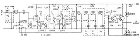
OPTOELECTRONIC_CHOPPER_WITH_NEONS
Published:2009/7/10 23:20:00 Author:May

Used with amplifier of sensitive potentiometer recorder.Diodes D1 and D2 short-circuit lamps on alternate half-cycles. Photoelectric chopping eliminates stray interference from a-c line and minimizes heat dissipation problems.-W.Moore,Photoconductors Chop D-C Signal levels,Electronics,38:9,p61-62 (View)
View full Circuit Diagram | Comments | Reading(536)
MAIN_GATE_MVBR_WITH_TRIODE_LIMITER
Published:2009/7/17 3:39:00 Author:Jessie

Triode connected to grid of normally-on tube limits swing of voltage. Plate of shutoff tube is tied to point in d-c coupling network between plate and grid, to give greater flexibility in setting plate voltage level of shutoff tube.-NBS, Handbook Preferred Circuits Navy Aeronautical Electronic Equipment, Vol. 1, Electron Tube Circuits, 1963, p N10-5. (View)
View full Circuit Diagram | Comments | Reading(557)
CALL_TONE_GENERATOR
Published:2009/7/10 23:19:00 Author:May

Amateur VHF relay stations are normally actuated by a 1750-Hz call tone. This might give problems if the relevant sending equipment has no internal call-tone generator, if it does not have sufficiently accurate frequencies, or if the tone duration is not long enough to securely energize the relevant relay.These problems can be overcome by the stand-alone generator described here. Simply placed in front of the microphone, it makes absolutely certain that the relay station is actuated. The generator consists of a quartz oscillator, a frequency counter and a buffer-amplifier-all contained in just two CMOS ICs. It is powered by a 9-V (p-p) battery, from which it draws a current of around 5 mA.Gates N1 and N2 form an oscillator that is controlled by a 3.27680-MHz crystal and provides clock pulses to IC2, which is connected as a programmable scaler. Diodes D1 through D5 determine the divide factor of 1872. Counter output Q1 provides the wanted 1 750-Hz signal, which is buffered by N3 through N6 before being applied to a piezoelectric buzzer. Capacitor C3 suppresses any harmonics, while R4 determines the volume of the output signal. (View)
View full Circuit Diagram | Comments | Reading(952)
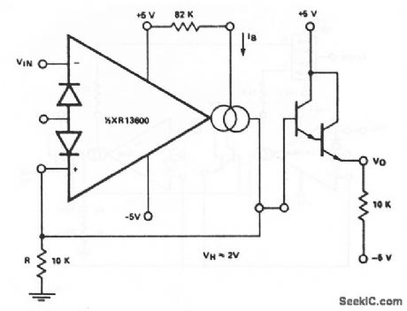
Tachometer
Published:2009/7/17 3:39:00 Author:Jessie

This circuit uses two sections of an XR-13600 (Fig. 11-1b) to form a tachometer or frequency-to-voltage converter. The input is triggered by a positive-going waveform. The maximum FIN is limited by the time required to charge Ct from VL to VH with a current of IB, where VL and VH represent the maximum-low and maximum-high output voltage swing of the XR-13600. D1 provides a discharge path for Ct when A1 switches low. EXAR Corporation Databook 1990 p 5-256 (View)
View full Circuit Diagram | Comments | Reading(2483)
TELEPHONE_VISUAL_RING_INDICATOR_1
Published:2009/7/10 23:16:00 Author:May

In this circuit, the ringing voltage on a telephone line causes NE-1 to break over, triggering SCR1, which in turn triggers SCR2. If a call has been received, depressing S2 will cause LED1 to light. Depressing S1 resets the circuit. This circuit has the advantage of lower battery drain because LED1 is not left on continuously after a ring signal, but only when S2 is depressed. (View)
View full Circuit Diagram | Comments | Reading(947)
MODEL_TRAIN_CROSSING_INCANDESCENT_FLASHER
Published:2009/7/17 3:38:00 Author:Jessie

This simple circuit can operate the incandescent bulbs in a railroad-crossing flasher. (View)
View full Circuit Diagram | Comments | Reading(728)
HYBRID_D_C_FEEDBACK_AMPLIFIER
Published:2009/7/10 23:14:00 Author:May
Used for calibrating a-c ammeters and voltmeters directly to standard cell.Use of tubes with chopper amplifier gives good temperature stability. Output to thermocouple is 7.5 ma.-E.A. Gilbert, Feedback Circuits for A-C Instrument Calibration,Electronics,33:40,p94-96 (View)
View full Circuit Diagram | Comments | Reading(574)
TUNNEL_DIODE_MONOSTABLE
Published:2009/7/17 3:38:00 Author:Jessie

Used as pulse-controlled oscillator. Power consumption is very low.- Transistor Manual, Seventh Edition, General Electric Co., 1964, p 366. (View)
View full Circuit Diagram | Comments | Reading(642)
EXTENSION_PHONE_RINGER
Published:2009/7/10 23:13:00 Author:May

The ac ringing voltage (typically 40 to 90 V at 26 Hz) is rectified by U1, the tone-ringer IC, and is used to drive that IC's internal tone-generator circuitry. The tone-generator IC includes a relaxation oscillator (with a base frequency of 500, 1 000, or 2 000 Hz) and frequency dividers that produce the high- and low-frequency tones, as well as the tone-warble frequency. An on-board amplifier feeds a 20-Vpp signal to the transducer. (View)
View full Circuit Diagram | Comments | Reading(1416)
Schmitt_trigger
Published:2009/7/17 3:37:00 Author:Jessie
This circuit uses one section of an XR-13600 (Fig. 11-1B) to form a Schmitt trigger. The circuit uses the amplifier output current into R to set the hysteresis of the comparator, thus producing a variable hysteresis, where VH = 2×R×IB . EXAR Corporation Databook 1990, p 5-256 (View)
View full Circuit Diagram | Comments | Reading(0)
12_conbattery_charger_with_20_ampere_PMS_maximum
Published:2009/7/17 3:37:00 Author:Jessie

12-conbattery charger with 20-ampere PMS maximum.ms circuits a simple relaxation oscillator using a UJT,The circuit will not work unless the polarity of the battery is observed when connected(courtesy Motorola Semiconductor Products Inc.). (View)
View full Circuit Diagram | Comments | Reading(825)
HIGH_POWER_ONE_SHOT
Published:2009/7/17 3:37:00 Author:Jessie

Operates from random-amplitude (10 to 28 V) square-wave input having 1 to 6.5 sec random duration, and switches 20-W load for adjustable period of 5 to 200 millisec. Can easily be adapted for transient detection, pulse-width adjustment, and time delays.-G. T. Pennell, High-Power One-Shot Multi, EEE, 12:9, p 62. (View)
View full Circuit Diagram | Comments | Reading(630)
SHUTTLE_TRACK_CONTROLLER
Published:2009/7/17 3:36:00 Author:Jessie

This circuit enables a model train to shuttle continuously between two tracks. When the train travels from left to right across the track in the lower part of the diagram, the lower rail (D) is connected to the positive supply line. After it has passed diode DB, the train will stop. Because the loco-motive short-circuits the diode when it passes the break in the rail, a short positive pulse is generated on rail section B. The pulse is used to set bistable IC1, whereupon D3 goes out and capacitor C3 is being charged. When the potential across the capacitor rises to a sufficiently high level, transistor T1 switches on, whereupon the relay is energized. This causes the polarity of rails C and D to be re-versed. Diode DB is then on, so the train departs in the direction of A. Rail C is then connected to the positive supply rail; so when the train passes diode DA, a positive pulse is generated on rail section A. This pulse is used to reset the biastable, whereupon the LED lights and the relay is deenergized. After the relay contacts have reversed the polarity of C and D again, diode DA comes on and the train departs again in the direction of B. (View)
View full Circuit Diagram | Comments | Reading(1419)
| Pages:795/2234 At 20781782783784785786787788789790791792793794795796797798799800Under 20 |
Circuit Categories
power supply circuit
Amplifier Circuit
Basic Circuit
LED and Light Circuit
Sensor Circuit
Signal Processing
Electrical Equipment Circuit
Control Circuit
Remote Control Circuit
A/D-D/A Converter Circuit
Audio Circuit
Measuring and Test Circuit
Communication Circuit
Computer-Related Circuit
555 Circuit
Automotive Circuit
Repairing Circuit