Signal Processing
80_AND_160_m_DIRECT_CONVERSION_RECEIVER
Published:2009/7/17 3:24:00 Author:Jessie | From:SeekIC


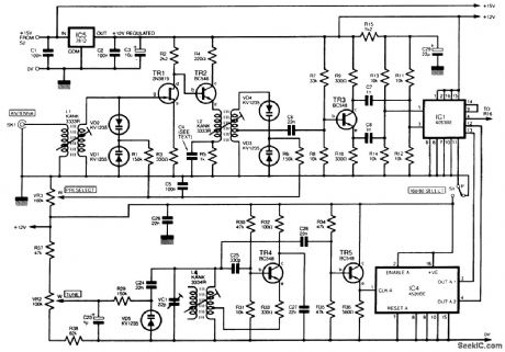
The full circuit diagram, except for power supply, for the direct-conversion top-band and 80-m receiver is shown. Incoming RF from the antenna is fed to the primary side of coil L1. This trans-former/coil is bought to resonance at the required frequency by a pair of back-to-back varicap diodes (VD1 and VD2). TRI, an RE, is coupled to the base (b) of transistor TR2, an emitter-follower. The output of TR2 feeds L2, the secondary being brought to resonance by varicaps VD3 and VD4. The variable-frequency oscillator (VFO) comprises a tuned circuit consisting of transformer L3, variable trimmer capacitor VC1, and varicap diode VD5. Variable bias to VD5 is provided by tuning control VR2. Transistor TR4 maintains oscillations at the desired frequency, and TR5 is an emitter-follower. The output of TR5 is sufficient to drive the CMOS divider chain formed by IC4. The VFO covers the frequency range 6.9 to 8.1 MHz, and this is divided by IC4 to produce 3450 to 4050 kHz for 80 m and 1725 to 2025 kHz for 160 m. The output of IC4 is fed to IC1, part of the product detector. The RF signal from the secondary tap on L2 is fed to a phase splitter formed around transistor TR3. Analog switch C1 operates at the selected VFO frequency and thus produces sum and difference frequencies of the VFO and the incoming RE. The output of IC1 at pin 4 is filtered to give resolved audio at this point. A high-gain inverting amplifier, with -3-dB points of approximately 300 Hz and 3 kHz, is formed by IC2a. This audio is now fed to IC3 with a maximum power output of 2 W. An LM380 is used in a standard configuration, and a fixed gain of around 30 dB is obtained.
Reprinted Url Of This Article:
http://www.seekic.com/circuit_diagram/Signal_Processing/80_AND_160_m_DIRECT_CONVERSION_RECEIVER.html
Print this Page | Comments | Reading(3)

Article Categories
power supply circuit
Amplifier Circuit
Basic Circuit
LED and Light Circuit
Sensor Circuit
Signal Processing
Electrical Equipment Circuit
Control Circuit
Remote Control Circuit
A/D-D/A Converter Circuit
Audio Circuit
Measuring and Test Circuit
Communication Circuit
Computer-Related Circuit
555 Circuit
Automotive Circuit
Repairing Circuit
Code: