
Circuit Diagram
Index 1214
50_54_MHz_RF_AGC_AMPLIFIER
Published:2009/6/30 22:20:00 Author:May
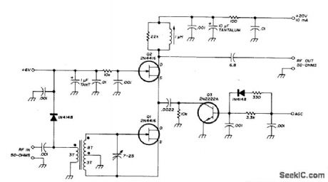
Developed for 6-roeter SSB transceiver to give minimum of 15-dB power gain, low noise figure, and good signal-handling capability when AGC is applied.AGC control resembles bipolar cascode drcuit using differential pair with current source, although operation does not involve changing amplifier bias Ievel. With increasing AGC voltage, a3 begins to turn on, shunting more and more signal cument away from 02 and thereby decreasing stage gain. Input transformer is wound on small toroid core. Range of AGO volt-age is 0-1.2 V.-A. Borsa, High-Performance BF-AGC Amplifier, Ham Radio, Sept. 1978, p 64-66. (View)
View full Circuit Diagram | Comments | Reading(2161)
LOW_PHASE_SHIFT
Published:2009/6/30 22:19:00 Author:May

Voltage-control led amplifier has less than 3°phase shift over gaincontrol range of 40 dB at frequencies up to 10 MHz, as required for AGO circuits. Current generator Q2 controls gain of wideband resistance-coupled amplifier Q1. Gain of al increases lineady with amplitude of positive control voltage on base of Q2.-A. H. Hargrove, Simple Circuits Control Phase-Shift, EDNMagazine, Jan, 1, 1971, p 39. (View)
View full Circuit Diagram | Comments | Reading(728)
TWO_DECADE_RANGE
Published:2009/6/30 22:17:00 Author:May
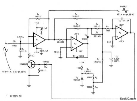
Output is maintained at 0.2V for inputs from 40mV to 4.1V. Voltage controlled JFET serves as variable control element. Comparator A3 produces error voltage that determines gain of A1, A2, and diodes form full-wave rectifier. Developed for use in radar seeker device to prevent overload of amplifier as target gets closer.-C. Marco, Automatic Gain Control oporates over Two Decades,Eleetriics, Aug,16、1973 p 99-100;reprinted in″Circuits for Electronics Engineers,″Electronics 1977、p 44-46 (View)
View full Circuit Diagram | Comments | Reading(558)
FET_GlVES_30_dB_GAIN_RANGE
Published:2009/6/30 22:16:00 Author:May
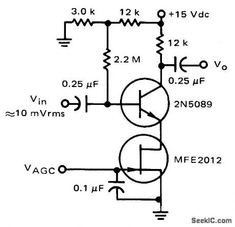
Only 1-V change in gate-source voltage of FET changes voltage gain over full range. Possible drawback is harmonic distortion due to unbypassed emit-ter degeneration.- Low Frequency Applica-tions of Field-Effect Transistors. Mototola, Phoenix, AZ, 1976, AN-511A, p 8. (View)
View full Circuit Diagram | Comments | Reading(495)
HANG_AGC
Published:2009/6/30 22:16:00 Author:May
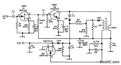
Provides very fast attack time with no AGC pop. Diodesare 1N914. When voltage across R10-08 decays below that across R9-C7, 03 conducts and clamps AGO bus to ground.AGO threshold is determined by value of RT, between 100K and 470K. AGC line must have high impedance, as with FET IF system. With l0 or bipolar IF amplifier, use low-impedance driver.T1 is audio transformer with 10K primary and 2K secondary (Radio Shack 273-1378).-D. Ste-vens, Solid-State Hang AGC, QST, July 1975, p 44. (View)
View full Circuit Diagram | Comments | Reading(1136)
AGC_WITH_CMOS_LOGIC
Published:2009/6/30 22:14:00 Author:May
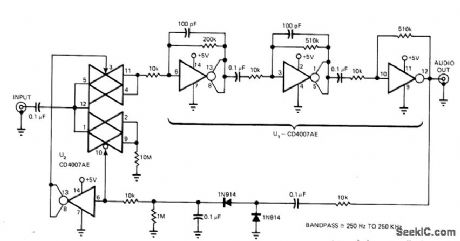
First stage U2, using CD4007AE, is wired as two-line demultiplexer with only one output acting as transmission gate. Gain is lower in first stage to reduce noise. U1 is used as three-stage high-gain audio amplifier in which first two stages have low-pass filtering for stability. AGO voltage, developed from audio output, is fed back to U, to turn transmission gate off when gain must be reduced. Audio output is about 2.5 V P-P for inputs of 2 mV and greater.-K. H. Fleischer, Tum Dig-ital CMOS IC's into a Low-Level AGC Amplifier, EDNMagazine, Oct.5,1977, p 99. (View)
View full Circuit Diagram | Comments | Reading(721)
AGC_WITH_MANUAL_CONTROL
Published:2009/6/30 22:13:00 Author:May

Used in 1.8-2 MHz communication receiver having wide dynamic range. R3 serves as manual IF gain control. R2 provides gain variation from 6 to 40 dB for AGO amplifier. Delay is about 1 s. Input is taken from primary of transformer that drives product detector of receiver, and AGC output goes to CA3028A IF opamp. Two-part article gives all other circuits of receiver.-D. DeMaw, His Eminence-the Receiver, QST, Part 2-July 1976, p 14-17 (Part 1-June 1976, p 27-30). (View)
View full Circuit Diagram | Comments | Reading(831)
AUDIBLE_S_METER
Published:2009/6/30 22:12:00 Author:May

When connected to repeater circuit generates tone burst 3 s after input signal has dropped out, with duration of 60 ms. Pitch of tone varies inversely with signal strength; highest pitch of 3500 Hz thus represents weak signal, and 350-Hz pitch corresponds to strongest input signal. Can be used to check performance of transmitters and antennas using that repeater. Repeater receiver must havesmeter, as in RCA CA3089E receiver, output of which can be fed to terminal A of circuit. Switch changes output from S-meter to audible encoder. Input B goes to squelch, C goes to +12 V source that is on when receiver is on, and D provides tone output for feed to audio amplifier and loudspeaker. Unlabeled transistors can be any medium-gain small-signal NPN and PNP silicon, comparable to European BC107 and BC177.-F. Johnson, Audible S-Meter for Repeaters, Ham Radio, March 1977, p 49-51. (View)
View full Circuit Diagram | Comments | Reading(770)
PEAK_PROGRAM_METER_TESTER
Published:2009/6/30 22:09:00 Author:May

Used with 5-kHz audio oscillator to produce tone bursts of 1.5,5,10,and 100 ms,as required for checking response of program meter to tone bursts.Transistors Tr3 and Tr, form mono with switched timing capadtors. Article covers calibration and use.-E. T. Garthwaite, Tone Burst Generator for Testing P P.Ms, Wireless World, Aug. 1976, p 53. (View)
View full Circuit Diagram | Comments | Reading(1104)
ECL_TTL_to_TTL_translator
Published:2009/7/24 9:34:00 Author:Jessie
This circuit adapts either ECL Or TTL circuits using an RC4508 comparator. Raytheon Linear Integrated Circuits, 1989, p. 5-14. (View)
View full Circuit Diagram | Comments | Reading(680)
AF_VOLTMETER
Published:2009/6/30 22:09:00 Author:May

Although not calibrated on absolute basis, either 3 dB or 10 dB of attenuation can be switched in with S1 for measuring purposes. Internal ad justments are made easily by tacking 51-ohm resistor temporarily across input, then driving input with step attenuator fed with audio power at -10 dB by generator having 50-ohm pad in its output. CR1-CR4 are 1N914.-W Hayward, Defining and Measuring Receiver Dynamic Range, 057, July 1975, p 15- 21 and 43. (View)
View full Circuit Diagram | Comments | Reading(903)
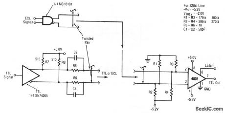
ECL_to_TTL_translator_tracking
Published:2009/7/24 9:32:00 Author:Jessie
This circuit uses an RC4508 comparator as an ECL-(single-ended) to-TTL translator with tracking ECL reference. Raytheon Linear Integrated Circuits, 1989, p. 5-13. (View)
View full Circuit Diagram | Comments | Reading(673)
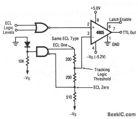
ECL_to_TTL_translator_extended_range
Published:2009/7/24 9:29:00 Author:Jessie

This circuit uses an RC4508 comparator as an ECL-to-TTL translator with extended common-mode range. Raytheon Linear Integrated Circuits, 1989, p. 5-13. (View)
View full Circuit Diagram | Comments | Reading(668)
MEASURING_AF_DISTORTION
Published:2009/6/30 22:08:00 Author:May
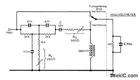
Passive highpass 1-kHz filter is used with audio millivoltmeter to improve accuracy of distortion measurements for low-impedance sources at 1 kHz.Filter removes low-frequency noise from input signal and compensates for loss of harmonic frequency. Applications include setting bias and recording levels of tape recorder. Adjust R1 for best null, then ad just R2 and value of C to equalize responses at harmonics.-J. B. Cole, Passive Network to Measure Distortion, Wireless World, Jan. 1978 p 60.
(View)
View full Circuit Diagram | Comments | Reading(545)
ECL_to_TTL_translator
Published:2009/7/24 9:26:00 Author:Jessie

This circuit uses an RC4508 comparator as an ECL-to-TTL translator. Raytheon Linear Integrated Circuits, 1989, p. 5-12. (View)
View full Circuit Diagram | Comments | Reading(966)
RTL_or_high_current_driver
Published:2009/7/24 9:24:00 Author:Jessie
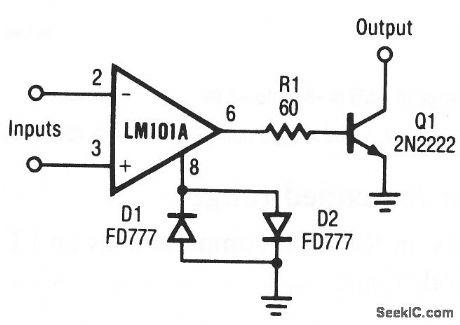
This circuit uses an LM101A as a voltage comparator to drive RTL or other high-current devices. Raytheon Linear Integrated Circuits, 1989, p. 4-247. (View)
View full Circuit Diagram | Comments | Reading(647)
AUDIO_FREQUENCY_METER
Published:2009/6/30 21:32:00 Author:May

Covers 0-100 kHz in four ranges. Meter reading is indepen-dent of signal amplitude frorn 1.7 VRMS upward and independent of waveform over wide range.Linear response means only one point need be calibrated in each frequency range. Circuit uses two overdriven FET amplifier stages in cascade.Square-wave output of Iast stage is rectified by X1 and X2. Deflection of meter depends only on number of pulses per second passing through meter so is proportional to pulse frequency.Battery drain is 1.4 mA.-R. P. Tumer, FET Cir-cuits, Howard W. Sams, Indianapolis, IN, 1977, 2nd Ed., p 129-131. (View)
View full Circuit Diagram | Comments | Reading(0)
DTL_TTL_driver
Published:2009/7/24 9:23:00 Author:Jessie

This circuit uses an LM101A as a voltage comparator to drive DTL/TTL ICs. Raytheon Linear Integrated Circuits, 1989, p. 4-247. (View)
View full Circuit Diagram | Comments | Reading(882)
-10_V_GIVES_10_kHz
Published:2009/6/30 21:31:00 Author:May


Control voltage input in range of 0 to -10 V is converted linearly to frequency of digital output pulse train haiving fullscale value of 10 kHz. Internal regulation of circuit makes operation essentially independent of ±15 V supply level.A1 is opamp integrator, A2 is comparator, and A3 is precision mono MVBR. Transistor switch Q1 connects Rb to 3.15-V reference voltage during t1 timing period of A3.—W.G.Jung, IC Timer Cookbook, Howard W.Sams, Indianapolis, IN, 1977, p184-192 (View)
View full Circuit Diagram | Comments | Reading(1330)
Basic_digital_D_A_converter
Published:2009/7/24 9:22:00 Author:Jessie

This circuit shows the classic DAC/op-amp combination that produces a digital D/A converter. VOUT is selected, in steps, by the binary signals at the digital input of DAC-10, with the highest VOUT set by VREF at pin 16. VREF is supplied by REF-01 (Fig.4-1). With the circuit assembled using the values shown (0.01 μF is typical for CC), apply binary inputs (typically -VS to -VS plus 36 V) at pins 5 through 14, stating with all zeros (or all 1s). Notice that VOUT varies (in steps) between 0 and a typical 9.9 V. Record actual values. Raytheon Linear Integrated Circuits, 1989, p. 495. (View)
View full Circuit Diagram | Comments | Reading(965)
| Pages:1214/2234 At 2012011202120312041205120612071208120912101211121212131214121512161217121812191220Under 20 |
Circuit Categories
power supply circuit
Amplifier Circuit
Basic Circuit
LED and Light Circuit
Sensor Circuit
Signal Processing
Electrical Equipment Circuit
Control Circuit
Remote Control Circuit
A/D-D/A Converter Circuit
Audio Circuit
Measuring and Test Circuit
Communication Circuit
Computer-Related Circuit
555 Circuit
Automotive Circuit
Repairing Circuit