
Circuit Diagram
Index 1209
Adjustable_LCD_supply_with_autotransformer
Published:2009/7/24 10:31:00 Author:Jessie
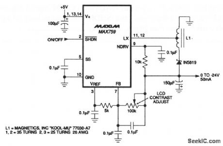
This circuit provides a variable output voltage to adjust the contrast of LCDs. The autotransformer L1 steps up the output to prevent overvoltage to the LX transistor. The total voltage from VIN to LX must be limited to 22 V (with a 5-V input), the voltage at LX cannot exceed -17 V. With L1 (a miniature 0.2-in diameter toroid), the voltage at LX is reduced from the output voltage (determined by the turns ratio). Maxim, 1992, Applications and Product Highlights, p. 4-5. (View)
View full Circuit Diagram | Comments | Reading(612)
15_V_LCD
Published:2009/6/30 23:48:00 Author:May

Will operate over 1 year on single 1.5-V AAA battery with accuracy of ±1 min. Basic timekeeping functions are provided by Motorola MC14440 CMOS device that includes calendar. 32.768-kHz NT-cut quartz crystal and trimming capacitor provide reference fre-quency. Output of 1.5-V alkaline cell is increased to 4 V for display by voltage tripler using MBD101 Schottky diodes.-J. Roy and A. Mou-ton, A Cordless, CMOS, Liquid-Crystal Display Clock, Motorola, Phoenix, AZ, 1977, EB-56. (View)
View full Circuit Diagram | Comments | Reading(1605)
8_digit_LED_driver
Published:2009/7/24 10:26:00 Author:Jessie
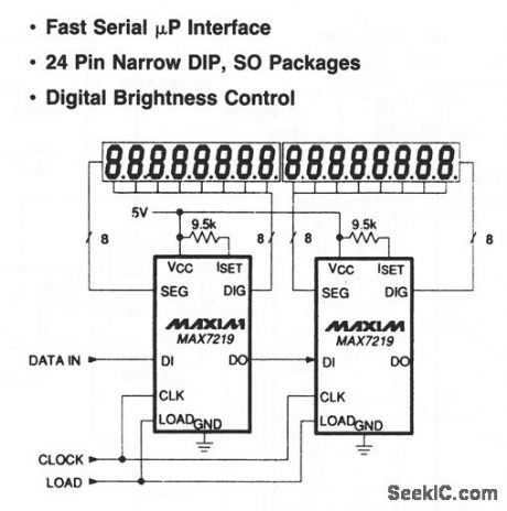
In this circuit, two MAX7217s drive 16 digits from a single 5-V supply, while being addressed through one 3-wire serial link. Only one external component (per chip) is needed. One resistor sets the maximum current (ISET) for all 8 segments, while a fast (up to 10 MHz) cascadable serial interface loads data directly from most microprocessors. Maxim, 1992, Applications and Product Highlights, p. 2-9. (View)
View full Circuit Diagram | Comments | Reading(741)
PHOTO_ALARM
Published:2009/6/30 23:47:00 Author:May

LDR1, a cadmium sulphide (CDS) photoresistive cell is used as the lower leg of a voltage divider between VCC and ground. The timer terminals 2 and 6 are connected to the junction of the photocell and SENSITIVITY control R1. The resistance of the photoresistive cell varies inversely as the light intensity; resistance is high when the illumination level' is low; low in bright light. (The Radio Shack CDS cell 276-116 has a typically wide resistance range-about 3 megohms in darkness and 100 ohms in bright light.) When the light is interrupted or falls below a level set by SENSITIVITY control R1, the rise in LDRl's resistance causes the voltage on pins 2 and 6 to rise. If the control is set so the voltage rises above 2/3 VCC, the relay pulls in. The relay drops out when the light level increases and the drop across the photocell falls below 2/3 VCC. (The circuit can be modified by placing relay K1 and diode Dl between pin 3 and ground. In this case, the relay drops out when the voltage on pins 2 and 6 rises above 2A Vgg, and pulls in when it falls below 1/3 VCC . This modification is valuable when the relay has single-throw contacts.) Opening and closing of the relay contacts occurs at different illumination levels. This 1/3 VCC hysteresis is an advantage that prevents the circuit from hunting and the relay from chattering when there are very small changes in illumination. (View)
View full Circuit Diagram | Comments | Reading(1067)
Isolated_D_A_converters_with_serial_input
Published:2009/7/24 10:24:00 Author:Jessie
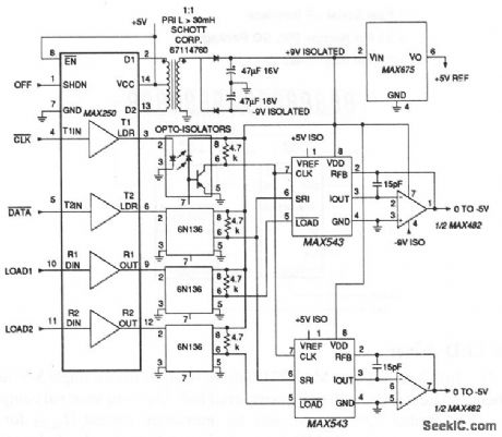
In this circuit, two MAX543 serial-input 12-bit D/A converters (DACs) receive power and data from a MAX250 receiver/transmitter. Clock and data lines are shared by both DACs, but separate LOAD1 and LOAD2 inputs latch the data in. The MAX250 also has a shutdown input (SHDN) that powers down the circuit and cuts supply current to less than 10μA. Maxim, 1992, Applications and Product Highlights, p. 2-9. (View)
View full Circuit Diagram | Comments | Reading(736)
A_D_converter_for_a_41_2_digit_LCD_display
Published:2009/7/24 10:19:00 Author:Jessie
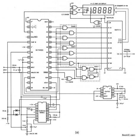
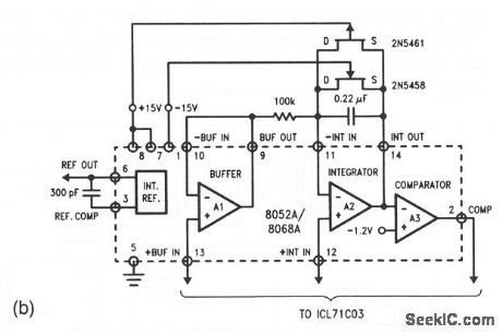
This circuit shows an ICL8052/ICL71C03 chip pair with an ICM7211 driver, which can be used to operate a 41/2-digit LCD display. With the values shown, the full-scale is ±2.000 V. Data bits are latched into the driver by the STROBE signal and Overrange is indicated by blinking the 4 digits. A 120-kHz clock is provided by an ICM7555. Figure 6-22B shows a gross overvoltage protection circuit (to be added if required). If the capacitor is added to put 36 of the ICM7211, the LCD backplane oscillator frequency is reduced from about 150 Hz. To adjust, short terminals 10 and 11 of the ICL71C03 and check that the display is 0000. Then, apply 2.000 V at terminals 10 and 11, and adjust the 10-kΩ potentiometer (pin 7 of the ICL71C03) for a reading of 2000 on the display. Harris Semiconductors, Data Acquisition, 1991, p. 2-25, 2-26. (View)
View full Circuit Diagram | Comments | Reading(2504)
VOLTAGE_TO_CURRENT_CONVERTERS
Published:2009/6/30 23:47:00 Author:May

A simple voltage-to-current converter is shown in the figure. The current out is IOUT or VIN/R. For negative currents, a pnp can be used and, for better accuracy, a Darlington pair can be substituted for the transistor. With careful design, this circuit can be used to control currents of many amps. Unity gain compen-sation is necessary. (View)
View full Circuit Diagram | Comments | Reading(5318)
CMOS_driver
Published:2009/7/24 9:36:00 Author:Jessie
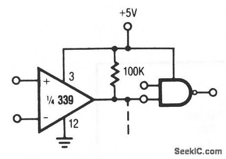
This circuituses a 339 comparator as a CMOS driver. Raytheon Linear Integrated Circuits, 1989, p. 5-30. (View)
View full Circuit Diagram | Comments | Reading(836)
+5_to__24_V_at_40_mA(with_low_power)inverter
Published:2009/7/24 9:03:00 Author:Jessie

This circuit is similar to that of Fig,4-60 In that the 2N4407 is a buffered replica of the MAX637 LX output.However,the 2N4407 has a high breakdown voltage and can be used to generate a-24-V output.The -24-V output does not appear directly on any pin of the MAX637 because it is sensed via the 1.5-MΩ external feedback resistor . (View)
View full Circuit Diagram | Comments | Reading(819)
Schmitt_trigger
Published:2009/7/24 9:02:00 Author:Jessie

This circuit is emitter coupled and provides a simple comparator action. The JFET places very little loading on the input. The 2N3565 bipolar is a high hFE transistor, so the circuit has fast transition action and a distinct hysteresis loop. National Semiconductor, Linear Applications Handbook, 1991, p. 118. (View)
View full Circuit Diagram | Comments | Reading(0)
ASTABLE_FLIP_FLOP_WITH_STARTER
Published:2009/6/30 23:47:00 Author:May


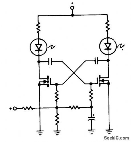
A pair of non-zenered MOSPOWER transistors, a pair of LEDs and a simple RC circuit make an easy sequential flasher with al-most unlimited sequencing time-from mo-mentary to several seconds. The infinite input resistance of the MOSFET gate allows for very long sequencing times that are impossible when using bipolars. One precaution, though, don't wire your circuit using phenolic or printed circuit boards when looking for slow sequencing (they exhibit too much leakage!). (View)
View full Circuit Diagram | Comments | Reading(973)
AUT0_CLOCK
Published:2009/6/30 23:46:00 Author:May
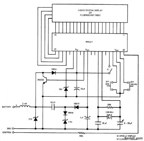
National MM5377 chip for au-tomobile dock interfaces directly with 4-digit Iiquid-crystal or fluorescent-tube display. 12-h format indudes Ieading-zero blanking and colon indication. Voltage-sensitive output drives energy-storage network serving as volt-age doubler/regulator. Crystal oscillator is ref-erence time base.- MOS/LSI Databook, Naˉtional Semiconductor,Santa Clara,CA,1977,1-33-1-37. (View)
View full Circuit Diagram | Comments | Reading(974)
AUDIBLE_DIPPER
Published:2009/6/30 23:45:00 Author:May
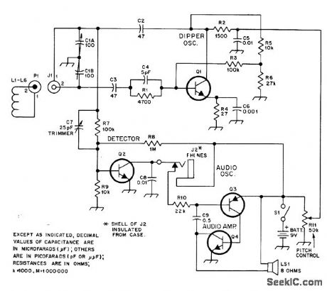
Designed for use by blind radio amateurs, but tone indication has advantage of permitting anyone to concentrate on equipment while checking antenna, tracking parasitics,or neutralizing amplifier with dip meter. Plug-in coils L1-L6 are Heathkit parts 40-1689 through 40-1695. Q1,Q2,and Q4 are Radio Shack RS-2021 or equivalent, and Q3 is RS-2021 or equivalent. Pitch of tone heard from Ioudspeakerdrops sharply when tuned circuit of dip-per becomes Ioaded by extemal source.-W. E.Quay,An Auditory Dip Oscillator, QST,Sept.1978,p25-27. (View)
View full Circuit Diagram | Comments | Reading(1887)
1_Hz_REFERENCE
Published:2009/6/30 23:44:00 Author:May
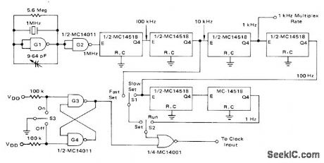
Output of 1-MHz crystal os-cillator is stepped down to 1 Hz by CMOS de-cade divider chain using Motorola MC14518 dual decade counters. Circuit also generates 1-kHz multiplex rate for display used with 24-h in-dustrial dock. Supply is +5 V.-D. Aldridge and A. Mouton, Industrial Clock/Timer Featuring Back-Up Power Supply Operation, Motorola, Phoenix, AZ, 1974, AN-718A, p 5. (View)
View full Circuit Diagram | Comments | Reading(913)
Step_up_down_dc_dc_converter
Published:2009/7/24 8:52:00 Author:Jessie

Positive-output step-up and step-down dc/dc converters have a common limitation in that neither can handle input voltages that can be both greater than (or less than) the output. For example, when convening a 12-V sealed lead-acid battery to a regulated + 12-V output, the battery voltage can vary from a high of 15 to 10 V. By using a MAX641 to drive separate P- and N-channel MOSFETs, both ends of the inductor are switched to allow noninverting buck/boost operation. A second advantage of the circuit over most boost-only designs is that the output goes to 0 V when Shutdown is activated. A drawback is that efficiency is not optimum because the two MOSFETs and diodes increase losses in the charge and discharge path of the inductor. The circuit delivers + 12 V at 100 mA with an 8-V input (70% efficiency). (View)
View full Circuit Diagram | Comments | Reading(1809)
VOLTAGE_TO_PULSE_DURATION_CONVERTER
Published:2009/6/30 23:44:00 Author:May

Voltage levels can be converted to pulse durations by combining an op amp and a timer IC. Accuracies to better than1% can be obtained with this circuit (a), and the output signals (b) still retain the original frequency, independent of the input voltage. (View)
View full Circuit Diagram | Comments | Reading(996)
Low_voltage_battery_to__5_V
Published:2009/7/24 8:50:00 Author:Jessie


By connecting a second inductor to the LX output of a MAX641 step-up dc/dc converter, the efficiency and power-handling ability can be dramatically improved. This circuit can supply 5 V at 40 mA with only 1.5-V input. With 2.4-V input, the circuit can supply 180 mA at 5 V. Notice that VOUT is not an output (in this circuit), but is the MAX641 voltage input. The pin is so labeled because VOUT is usually the output/feedback terminal of a stand-alone MAX641. (View)
View full Circuit Diagram | Comments | Reading(822)
High_voltage_step_up_converter
Published:2009/7/24 8:49:00 Author:Jessie

In this circuit, a +12-V input is converted to a +50 V at 50 mA by adding an IRF530 N-channel FET, which has a voltage rating of 100 V. The circuit differs from the basic MAX641 hookup in that an external resistor-divider must provide the feedback to the VFB input and that chip power comes from the + 12-V input via the VOUT pin. (View)
View full Circuit Diagram | Comments | Reading(1905)
SEQUENTIAL_AC_FLASHER
Published:2009/6/30 23:42:00 Author:May

This circuit uses a ring counter made up of Q3, Q4 and Q5. Q2 acts as an oscillator which triggers the SCRs Q3, Q4 and Q5 in sequence. When an SCR fires, a 0.2μF ca-pacitor provides commutation, shutting off the previous stage. Triacs Q6, Q7 and Q8 control lamps 1, 2 and 3 respectively. (View)
View full Circuit Diagram | Comments | Reading(0)
Medium_power_step_up_converters
Published:2009/7/24 8:47:00 Author:Jessie

The table of Fig. 4-53B lists measured efficiency of circuits using the indicated coils. In selecting coils for circuits that use external MOSFETs, it is important to calculate the peak current and to select a coil that will not saturate at that peak current. (View)
View full Circuit Diagram | Comments | Reading(1084)
| Pages:1209/2234 At 2012011202120312041205120612071208120912101211121212131214121512161217121812191220Under 20 |
Circuit Categories
power supply circuit
Amplifier Circuit
Basic Circuit
LED and Light Circuit
Sensor Circuit
Signal Processing
Electrical Equipment Circuit
Control Circuit
Remote Control Circuit
A/D-D/A Converter Circuit
Audio Circuit
Measuring and Test Circuit
Communication Circuit
Computer-Related Circuit
555 Circuit
Automotive Circuit
Repairing Circuit