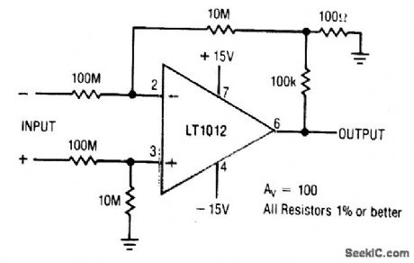
Circuit Diagram
Index 1205
INSTRUMENTATION_AMPLIFIER_WITH_±100_VOLT_COMMON_MODE_RANGE
Published:2009/7/1 1:00:00 Author:May
View full Circuit Diagram | Comments | Reading(458)
Low_cost_buck_regulator
Published:2009/7/24 5:44:00 Author:Jessie

This low-cost circuit provides line regulation (at a value set by D1) with a minimum of components. Typical values for Cin, and Co are 500μF. (View)
View full Circuit Diagram | Comments | Reading(823)
INSTRUMENT_PREAMP
Published:2009/7/1 0:59:00 Author:May

The input impedance is the value of potentiometer R1. If your instrument has extra-deep bass, change capacitor C1 to 0.5 μF. What appears to be an extra part in the feedback loop is a brightening tone control. The basic feedback from the op amp's output (pin 6) to the inverting input (pin 2) consists of resistor R7, and the series connection of resistor R4 and capacitor C3, which produce a voltage gain of almost 5 (almost 14 dB). That should be more extra oomph than usually needed. If the circuit is somewhat short on bass response, increase the value of capacitor C3 to 1 to 10μF. Start with 1 μF and increase the valud until you get the bass effect you want. (View)
View full Circuit Diagram | Comments | Reading(1757)
Boost_switching_regulator
Published:2009/7/24 5:43:00 Author:Jessie

This circuit provides an output (+24 V) that is double the input (+ 12 V). (View)
View full Circuit Diagram | Comments | Reading(854)
Negative_voltage_flyback_regulator
Published:2009/7/24 5:42:00 Author:Jessie

This circuit provides a negative output (-5 V) with a positive input (+12 V). (View)
View full Circuit Diagram | Comments | Reading(785)
PLANT_WATER_MONITOR
Published:2009/7/1 0:58:00 Author:May
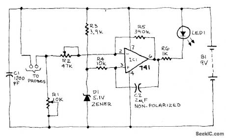
When the soil is moist, the LED glows. If the moisture falls below a certain predetermined level, the LED begins to flash. If there is still less moisture, the LED tums off. To calibrate, connect the battery and insert the probe into a container of dry soil. Set R1 to its maximum value then reduce that resistance until the LED begins to flash. The range over which the LED flashes before going out is adjusted using R2. (View)
View full Circuit Diagram | Comments | Reading(872)
High_voltage_negative_switching_regulator
Published:2009/7/24 5:41:00 Author:Jessie

The characteristics of this circuit are the same as in Fig, 4-26, except that the input can exceed 40 V, and the input/output is negative. (View)
View full Circuit Diagram | Comments | Reading(589)
High_voltage_positive_switching_regulator
Published:2009/7/24 5:39:00 Author:Jessie

The characteristics of this circuit are the same as in Fig. 4-26, except that the input can exceed 40 V. (View)
View full Circuit Diagram | Comments | Reading(577)
Alternate_positive_voltage_switching_regulator
Published:2009/7/24 5:38:00 Author:Jessie

The input and output characteristics of this circuit are the same as in Fig. 4-26, except that a μA723 is used instead of an LM305. Notice that a 2N2222 is required for Q 1 . (View)
View full Circuit Diagram | Comments | Reading(460)
Negative_voltage_switching_regulator
Published:2009/7/24 5:36:00 Author:Jessie

The input and output characteristics of this circuit are the same as in Fig. 4-26, except that input and output are negative. (View)
View full Circuit Diagram | Comments | Reading(621)
PULSED_INFRARED_DIODE_EMITTER_DRIVE
Published:2009/7/1 0:57:00 Author:May
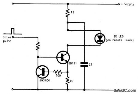
Q1 and Q2 form a constant current drive defmed by R2. (I approximates to the reciprocal of R2 in the circuit shown for values of I greater than 1 amp). The pulse current is drawn from C1 which is recharged during the time between pulses via R1. The value of C1 is determined from the duration and magnitude of the peak current required, and the time constant R1 C1 is determined from the duration between pulses. (View)
View full Circuit Diagram | Comments | Reading(669)
Slew_rate_reduction_for_high_crryoacity_loads
Published:2009/7/24 5:36:00 Author:Jessie

Figure 8-50 shows a method for reducing the slew rate in the circuits of Figs. 8-48 and 8-49. Supply circuits in battery-operated equipment are often bypassed with large capacitors to reduce transients. If not properly switched, such filter capacitors can produce glitches at start-up. For example, the 100-μF load capacitance shown could easily produce a start-up current of 10 A (well beyond the capability of the regulator), and possibly prevent start-up. The circuit of Fig. 8-50 reduces start-up current to about 15 mA. LINEAR TECHNOLOGY, APPLICATION NorE 53, P. 3. (View)
View full Circuit Diagram | Comments | Reading(651)
Positive_voltage_switching_regulator
Published:2009/7/24 5:35:00 Author:Jessie

With the values shown, this circuit produces a±5-V output (± 1%), with a 20- to 40-V input, at currents between 2 and 10 A. mVpp (View)
View full Circuit Diagram | Comments | Reading(634)
Quartz_stabilized_bridge_oscillator_with_sine_wave_output
Published:2009/7/24 5:35:00 Author:Jessie

Figure-26 shows a crystal-controlled bridge-based oscillator, where one leg of the bridge is formed by a lamp(a classic circuit).Figure 4-27 shows the waveforms,As the oscillation amplitude builds, the lamp current increases, as does lamp resistance. This causes a reduction in gain, and the circuit finds a stable operating point, The 15-pF capacitor suppresses Spurious oscillation. The amplifier output(trace A, Fig,4-27)is a sine wave without about 1.5%distortion(trace B),caused primarily by common-mode swing,LINEAR TECHNOLOGY,APPLICATION NOTE 43,P. 28. (View)
View full Circuit Diagram | Comments | Reading(585)
INFRARED_RECEIVER
Published:2009/7/1 0:56:00 Author:May
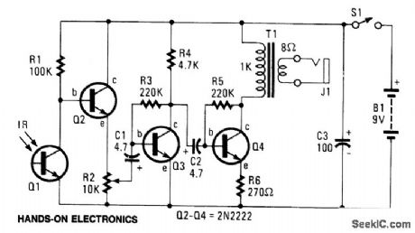
The circuit consists of Q1-a phototransistor that responds to an intensity of amplitude-modulated IR light source-and a three-stage, high-gain audio amplifier.Transformer T1 is used to match the output impedance of the receiver to today's popular low-impedance (low-Z) headphones; but if a set of 1000-2000 ohm, magnetic (not crystal), high-impedance (high-Z) phones are to be used, remove T1 and connect the high-Z phones in place of T1's primary winding-the 1000-ohm winding. (View)
View full Circuit Diagram | Comments | Reading(1950)
Dual_high_side_switch_driver_with_extended_voltage_range
Published:2009/7/24 5:34:00 Author:Jessie

Figure 8-49 shows an LTC1155 connected as a switch driver for voltages greater than 9 V. The circuit is the same as that shown in Fig. 8-48, with the addition of the zeners. LINEAR TECHNOLOGY, APPLICATION NOTE 53, P. 2. (View)
View full Circuit Diagram | Comments | Reading(622)
INVISIBLE_INFRARED_PULSED_LASER_RIFLE
Published:2009/7/1 0:55:00 Author:May
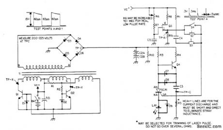
The device generates an adjustable frequency of low to medium powered IR pulses of invisible energy and must be treated with care.The portable battery pack is stepped up to 200 to 300 volts by the inverter circuit consisting of Q1, Q2, and T1. Q1 conducts until saturated, at which time, the base no longer can sustain it in an on state and Q1 turns off, causing the magnetic field in its collector winding to collapse thus producing a voltage or proper phase in the base drive winding that turns on Q2 until saturated, repeating the above sequence of events in an on/off action. The diodes connected at the bases provide a return path for the base drive current. The stepped up squarewave voltage on the secondary of T1 is rectified and integrated on C2. (View)
View full Circuit Diagram | Comments | Reading(527)
Dc_dc_converter_without_external_sync
Published:2009/7/24 5:34:00 Author:Jessie

This circuit is similar to that of Figs. 4-22 and 4-24, except that there is no provision for extenal sync. The input voltage is 15 to 70 V. Typical maximum loads are 167 mA at +5V, and 33 mA at -5V. Typical minimum loads are 32 mA at + 5 V and 8 mA at -5 V. Maximum ripple is 100 mVpp. Regulation is ±5%. L1 is any 100-μH 75-mA inductor. L2 is GFS Manufacturing #85-787-4. (View)
View full Circuit Diagram | Comments | Reading(744)
INFRARED_TRANSMITTER_1
Published:2009/7/1 0:54:00 Author:May
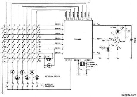
The transmitter keyboard is arranged as a scanned matrix. The matrix consists of 7 driver outputs and 7 sense inputs. The driver outputs DRVON to DRV6N are open-drain n-channel transistors and they are conductive in the stand-by mode. The 7 sense inputs (SENON to SEN6N) enable the generation of 56 command codes. With 2 external diodes all 64 commands are addressable. The sense inputs have p-channel pull-up transistors, so that they are HIGH until they are pulled LOW by connecting them to an output via a key depression to initiate a code transmission. (View)
View full Circuit Diagram | Comments | Reading(0)
Temperature__compensated_crystal_oscillator_TCXO
Published:2009/7/24 8:01:00 Author:Jessie
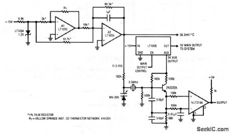
This circuit shows a temperature-controlled crystal oscillator without an expensive, power-consuming oven. Instead, the crystal frequency is controlled by an MV-209 varactor. In turn, the MV209 is controlled by a linear thermistor in the feedback loop of A1. Linear Technology Corporaton. Linear Appications Handbook, 1990, p. AN12-4. (View)
View full Circuit Diagram | Comments | Reading(1016)
| Pages:1205/2234 At 2012011202120312041205120612071208120912101211121212131214121512161217121812191220Under 20 |
Circuit Categories
power supply circuit
Amplifier Circuit
Basic Circuit
LED and Light Circuit
Sensor Circuit
Signal Processing
Electrical Equipment Circuit
Control Circuit
Remote Control Circuit
A/D-D/A Converter Circuit
Audio Circuit
Measuring and Test Circuit
Communication Circuit
Computer-Related Circuit
555 Circuit
Automotive Circuit
Repairing Circuit
