
Circuit Diagram
Index 1204
Voltage_controlled_crystal_oscillator_VCXO
Published:2009/7/24 8:07:00 Author:Jessie

This circuit shows a voltage-controlled crystal oscillator. Figure 5-33B shows the tuning characteristics (frequency shift versus tuning voltage). Linear Technology Corporation, Linear Appications Handbook, 1990, p. AN12-5. (View)
View full Circuit Diagram | Comments | Reading(1423)
Dual_high_side_switch_driver
Published:2009/7/24 5:33:00 Author:Jessie

Figure 8-48 shows an LTC1155 connected as a high-side MOSFET switch driver (Chapter 2). The circuit generate 12-V from a 5-V supply to fully enhance (switch) logic-level N-channel MOSFET switches, with no external components required. The supply current is typically 85 μA with the switch fully enhanced, and 8 μA with the LTC1155 in standby (both inputs off). This combination of a low-drop N-channel MOSFET switch and micropower driver is an efficient means of controlling power in complex loads. Switch efficiencies in the 99% range are practical. LINEAR TECHNOLOGY, APPUCAnON NOTE 53, p. 1. (View)
View full Circuit Diagram | Comments | Reading(1363)
Quartz_stabilized_bridge_oscillator
Published:2009/7/24 5:33:00 Author:Jessie
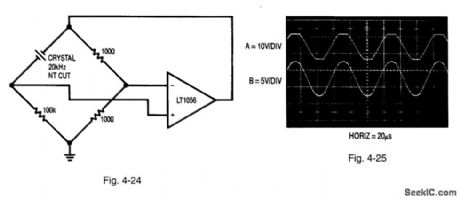
Figure 4-24 shows a bridge-based oscillator, where one leg of the bridge is replaced with a resonant element. Figure 4-25 shows the waveforms. With the crystal removed, the circuit is a basic non-inverting gain-of-two amplifier with grounded input. Inserting the crystal closes a positive-feedback path at the crystal resonant frequency. The amplifier output (trace A, Fig. 4-25) swings in an attempt to maintain input balance. Excessive circuit gain prevents linear operation, and oscillations start when the amplifier repeatedly overshoots in an attempt to null the bridge. The high Q of the crystal is evident in the filtered waveform (trace B) at the amplifier positive input. LINEAR TECHNOLOGY APPLICATION NOTE 43, P. 27. (View)
View full Circuit Diagram | Comments | Reading(560)
Bridge_oscillator_with_square_wave_output
Published:2009/7/24 5:33:00 Author:Jessie
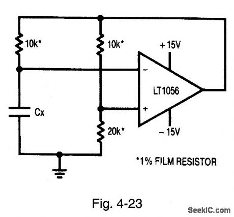
Figure 4-23 shows an oscillator circuit formed from the circuit of Fig. 4-22. In effect, the Fig. 4-23 circuit is a classic op-amp multivibrator (MV). The 10-kΩ/20-kΩ bridge leg provide switching-point hysteresis, with Cx charged through the remaining 10-kO resistor. When Cx reaches the switching point, the amplifier output changes state, abruptly reversing the sign of the positive output. The charging direction of Cx, also reverses to sustain oscillation. Output frequency depends on bridge components (at frequencies that are low compared to amplifier delays). Amplifier input errors tend to cancel, and supply shifts are generally rejected. The duty cycle is influenced by output saturation and supply asymmetry. LINEAR TECHNOLOGY, APPLICATION NOTE 43, P. 27. (View)
View full Circuit Diagram | Comments | Reading(625)
Dc_dc_converter_1
Published:2009/7/24 5:33:00 Author:Jessie

This circuit is similar to that of Fig. 4-22, except that a 3-W Si9100 is used instead of a 1-W Si9105 as the switchmode regulator. Notice that the sync input (at pins 7 and 8) is optional for both circuits. (View)
View full Circuit Diagram | Comments | Reading(616)
LCD-contrast_supply_for_color_displays
Published:2009/7/24 5:32:00 Author:Jessie

Figure 8-46 shows a MAX641 connected as an LCD-contrast supply with positive26-V to 38-V output (primarily for color displays). Figure 8-47 shows the efficiencycurves.The circuit operates over a 4.5-V to 15-V(five-to eight-cell)range, draws550 μA (with 5-V in and 26-V output) or 1-mA (with 9.6-V input and 38-V output) quiescent current and is capable of 30-mA output,Load regulation is 0.16%/mA, line regulation is 0.16%/V output. and output noise is 200 mV p-p.The input range makesthe circuit suitable for+5 -V regulated input or for a direct-battery connection. For input voltages above 7 V substitute a 100-μH inductor (Coiltronix CTS100-4) to maintain low output nolse and ripple.MAXIM BATTERY MANAGEMENT CIRCUITCOLLECTION. 1994 P.50. (View)
View full Circuit Diagram | Comments | Reading(580)
MACHINE_VISION_ILLUMINATION_STABILIZER
Published:2009/7/1 1:13:00 Author:May
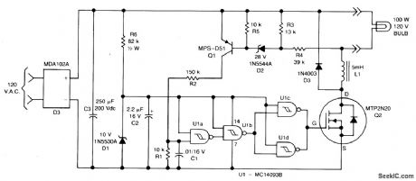
The combination of Q1, Q2 and U1 form a hysteresis oscillator to stabilize lamp illumination. In operation, full wave bridge D3 operates directly from the ac line to sup-ply unregulated dc to the lamp and also to the 10 V zener that provides power to the quad CMOS Schmitt trigger, U1. When the lamp supply exceeds 115 V, Q1 is turned ON, charging Ct through R2 to raise the input to Ula past the positive-going logic thresh-old. This drops the output voltage at Ulc and Uld, which drives the gate of Q2, turning it OFF. Current then decays through the lamp, L1 and D3 until the lamp voltage falls below 115 V, at which time Q1 turns OFF and the cycle repeats. (View)
View full Circuit Diagram | Comments | Reading(662)
Time_domain_bridge
Published:2009/7/24 5:31:00 Author:Jessie


Figure 4-22 shows a bridge circuit that operates in the time domain, and is particularly suitable for capacitance measurement. With S1 closed, the comparator output is high. When S1 opens, capacitance Cx charges. When the Cx potential crosses the voltage established at the comparator noninverting input, the comparator output goes low. The elapsed time between the switch opening and the comparator going low is proportionate to the Cx, value. The circuit is insensitive to supply and repetition rate variations, and can provide good accuracy if the time constants are kept much larger than comparator and switch delays. The LT1011 delay is about 200 ns, and the LTC201A delay is about 450 ns. To ensure 1% accuracy, the time constant of Cx and the series resistor should not go below 65 μs.Extremely low values of capacitance might be influenced by switch charge injection.In such cases, switching should be implemented by alternating the bridge drive between ground and +15 V. LINEAR TECHNOLOGY, APPLICAION NOTE 43, P. 27. (View)
View full Circuit Diagram | Comments | Reading(762)
Dc_dc_forward_converter
Published:2009/7/24 5:30:00 Author:Jessie

The feedback isolation circuit (shown within the box) can be replaced by the simple R7/R8 voltage feedback divider if the supply-output feedback does not need to be isolated from the load. (View)
View full Circuit Diagram | Comments | Reading(688)
SINGLE_CHIP_PUMP_CONTROLLER
Published:2009/7/1 1:12:00 Author:May

This circuit controls the level of a tank using a bang-bang controlled electrical pump.The actual level of liquid is measured by a capacitive level-meter. The first inverter performs as a capacitance to frequency converter. It is a Schmitt oscillator and its frequency output decreases as the capacitance increases. The second inverter is a monostable which performs as a frequency to voltage converter (f/V). Its output is applied to the maximum and minimum level comparator inputs. Maximum and minimum liquid levels may be set by the potentiometers. The maximum level (1 max) may be preset between the limits: 65 pF less than C (1 max) less than 120 pF. The minimum level is presetable and the limits are: 0 less than C (1 min) less than 25 pF. (View)
View full Circuit Diagram | Comments | Reading(912)
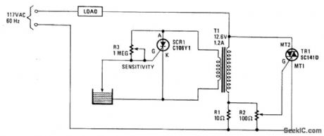
VOLTAGE_REGULATOR_FOR_A_PROJECTION_LAMP
Published:2009/7/1 1:12:00 Author:May
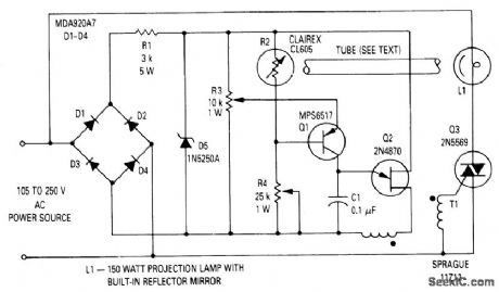
The circuit will regulate the rms output voltage across the load (a projection lamp) to 100 volts 12% for an input voltage between 105 and 250 volts ac. This is accom-plished by indirectly sensing the light output of lamp L1 and applying this feedback signal to the firing circuit (Q1 and Q2) which controls the conduction angle of TRIAC Q3. The lamp voltage is provided by TRIAC Q3, whose conduction angle is set by the firing circuit for unijunction transistor Q2. The circuit is synchronized with the line through the full-wave bridge rectifier. The voltage to the firing circuit is limited by zener diode D5. Phase control of the supply voltage is set by the charging rate of capacitor C1. Q2 will fire when the voltage on C1 reaches approximately 0.65 times the zener voltage. The charging rate of C1 is set by the conduction of Q1, which is controlled by the resistance of photocell R2. Potentiometers R3 and R4 are used to set the lamp voltage to 100 volts when the line voltage is 105 volts and 250 volts, respectively. (View)
View full Circuit Diagram | Comments | Reading(1264)
PAFITY_LINE_INTERCOM
Published:2009/7/1 1:10:00 Author:May
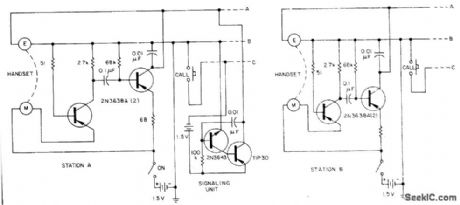
A large number of intercom stations can be tied together. All units are connected in parallel, and the entire system is buzzed by only one signaling circuit. Each unit is powered individually from 1.5-V cells for redundancy. For greater signal volume, 3-V sources can be used for the supplies without changing any other parts of the system. The carbon microphone of a standard telephone handset at each station feeds into a common-base amplifier, and a tandem high-gain common-emitter stage drives the intercom line. All phone earpieces are in parallel across the line. The signaling circuit, also connected across the line, is a simple oscillator that drives all the earpieces. (View)
View full Circuit Diagram | Comments | Reading(623)
INTERCOM
Published:2009/7/1 1:09:00 Author:May
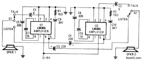
The circuit consists of separate amplifiers-one for each station-rather than a single amplifier and a time sharing arrangement. U1 and U2 are low-voltage audio amplifiers, each of which operates as separate entities with switches at either station controlling which will transmit or receive. With capacitors C7 and C8 included in the circuit, the amplifiers have a gain of 200. Omitting those two components drops the gain to about 20. Other gain levels are available with the addition of a series-connected R/C combination connected between pin 1 and pin 8-for example, a 1000 ohm resistor and 10 μF capaci-tor for a gain of about 150. (View)
View full Circuit Diagram | Comments | Reading(1879)
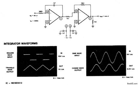
LONG_TIME_INTEGRATOR
Published:2009/7/1 1:07:00 Author:May

View full Circuit Diagram | Comments | Reading(629)
ACTIVE_INTEGRATOR_WITH_INVERTING_BUFFER
Published:2009/7/1 1:07:00 Author:May
View full Circuit Diagram | Comments | Reading(683)
WATER_LEVEL_SENSING_AND_CONTROL
Published:2009/7/1 1:06:00 Author:May
The operation of the circuit is based on the difference in the primary impedance of a transformer when its secondary is loaded and when it is open-circuit. The impedance of the primary of T1 and resistor R1 are in series with the load. The triac's gate-control voltage is developed across parallel resistors R1 and R2. When the water level is low, the probe is out of the water and SCR1 is triggered on. It conducts and imposes a heavy load on transformer T1's secondary winding. That load is reflected back into the primary, gating triac TR1 on, which energizes the load. If the load is an electric value in the water-supply line, it will open and remain open until the water rises and touches the probe, which shorts SCRl's gate and cathode, thereby turning off the SCR1, which effectively open-circuits the secondary. The open-circuit condition-when reflected back to the primary winding-removes the triac's trigger signal, thereby turning the water off. The load may range from a water valve, a relay controlling a pump supplying water for irrigation, or a solenoid valve controlling the water level in a garden lily pond. (View)
View full Circuit Diagram | Comments | Reading(1455)
IMPROVED_NON_INVERTING_INTEGRATOR
Published:2009/7/1 1:06:00 Author:May
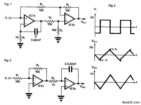
In the circuit in Fig. 1, IC1a produces the integral term required but also has the side effect of producing a proportional term not required, so this term is subtracted by IC1b leaving a pure integral. If the ratio R2/R5 does not exactly match the ratio of R3/R4, the subtraction will not be complete and a small amount of the proportional term will reach the output. The result of this with a squarewave input is shown in Fig. 3a as small steps in the output waveform at points X and Y.This effect can be completely removed by using the simplified circuit shown in Fig.2. Here the signal is pre-inverted by IC1a, then fed to a standard inverting integrator IC1b. The result is a non-inverting integrator with the advantage that the unwanted proportional term is never produced, so it does not need to be subtracted. (View)
View full Circuit Diagram | Comments | Reading(2446)
SATURATED_STANDARD_CELL_AMPLIFIER
Published:2009/7/1 1:04:00 Author:May

View full Circuit Diagram | Comments | Reading(530)
INSTRUMENTATION_METER_DRIVER
Published:2009/7/1 1:04:00 Author:May

Three op amps U1, U2, and U3 are connected in the basic instrumentation amplifier configuration. Operating from ±5 V, pin 8 of each op amp is connected directly to ground and provides the ac performance desired in this application (high bias mode). P1 is for offset error correction and P2 allows adjustment of the input common mode rejection ratio. The high input impedance allows megohms without loading. The resulting circuit frequency response is 200 kHz at -3 dB and has a slew rate of 4.5 V/μs. (View)
View full Circuit Diagram | Comments | Reading(1445)
CURRENT_COLLECTOR_HEAD_AMPLIFIER
Published:2009/7/1 1:02:00 Author:May

To amplify small current signals such as from an electron-collector inside a vacuum chamber, it is convenient for reasons of noise and bandwidth to have a head-amplifler: ' attached to the chamber. The op amp N1 is a precision bipolar device with extremely low bias current and offset voltage (1) as well as low noise, which allows the 100:1 feedback attenuator R4:R5. The resistance of R3 can be varied from above 10M to below 1R, and so the nominal 0 to 1 V-peak output signal corresponds to input current ranges of 1 nA to 10 μA, this current i enters via the protective resistor R1. Light from the bulb BI shines on R3, and the filament current I is controlled by the op amp N2.The reference voltage VR is shaped by the resistors R9R10 so as to tailor the bulb and LDR characteristics to the desired current ranges. Thus, rotation of the calibrated knob K gives the appropriate resistance to R3 for the peak-current scale shown. (View)
View full Circuit Diagram | Comments | Reading(622)
| Pages:1204/2234 At 2012011202120312041205120612071208120912101211121212131214121512161217121812191220Under 20 |
Circuit Categories
power supply circuit
Amplifier Circuit
Basic Circuit
LED and Light Circuit
Sensor Circuit
Signal Processing
Electrical Equipment Circuit
Control Circuit
Remote Control Circuit
A/D-D/A Converter Circuit
Audio Circuit
Measuring and Test Circuit
Communication Circuit
Computer-Related Circuit
555 Circuit
Automotive Circuit
Repairing Circuit