
Circuit Diagram
Index 1216
Digital_power_monitor
Published:2009/7/24 12:03:00 Author:Jessie
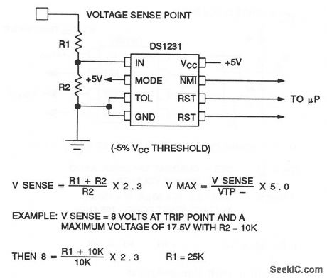
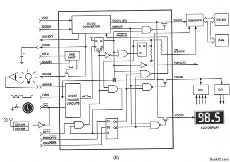
This circuit shows a DS1231 power monitor chip that is used to control a digital-system power supply. The DS1231 uses a temperature-compensated reference circuit to provide both an orderly shutdown and automatic restart of processor-based systems. The DS1231 operates by monitoring the high-voltage inputs to the power-supply regulators (at a voltage sense point), and applying RST or RST and NMI (nonmaskable interrupt) control signals to the processor. The time for processor shutdown is directly proportional to the available hold-up time of the power supply. Just before the hold-up time is exhausted, the DS1231 unconditionally halts the processor (to prevent spurious cycles) by enabling reset when VCC falls below a selectable 5 or 10% threshold. Notice that the TOL pin is grounded for a 5% threshold. When power returns, the processor is held inactive until well after power conditions have stabilized, safeguarding any nonvolatile memory in the system from inadvertent data changes. Dallas Semiconductors, Product Data Book, 1992/1993, p. 10-40. (View)
View full Circuit Diagram | Comments | Reading(761)
RS_232_transmitter_receiver_with_external_power
Published:2009/7/24 11:59:00 Author:Jessie
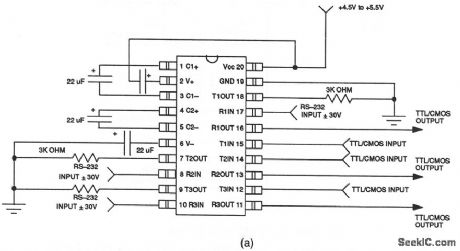
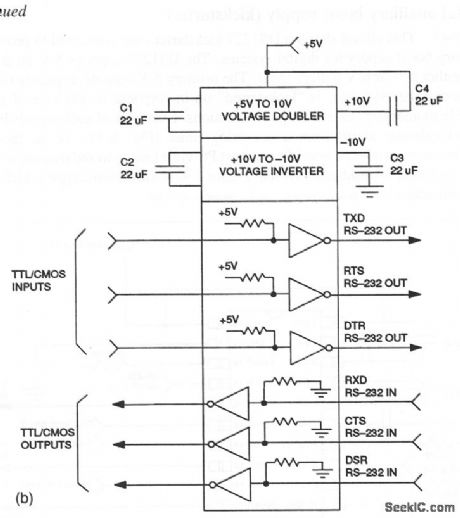
This circuit shows a DS1229 that is connected as a triple RS-232 transmitter/receiver. The DS1229 has two internal charge pumps that are used to generate ±10 V, and six level translators. Three of the translators are RS-232 that convert TTL/CMOS inputs into +9-V RS-232 outputs. The other three translators are RS-232 receivers that convert RS-232 inputs to 5-V TTL/CMOS outputs. Figurd 6-46B shows some typical RS-232 interconnections. Dallas Semiconductors, Product Data Book, 1992/1993, p. 10-33, 10-34. (View)
View full Circuit Diagram | Comments | Reading(641)
Digital_auxiliary_boost_supply_kickstarter
Published:2009/7/24 11:56:00 Author:Jessie
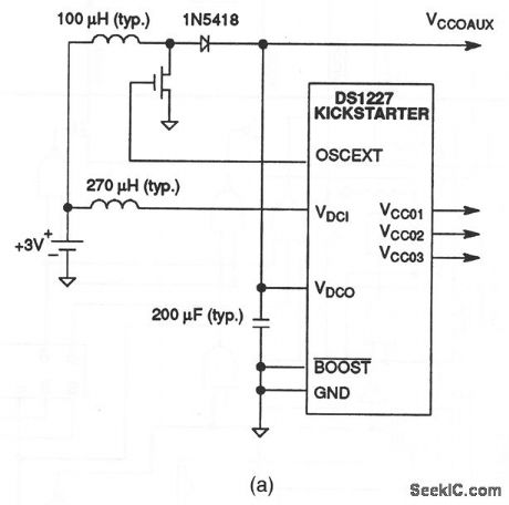
This circuit shows a DS1227 kickstarter chip connected to provide an auxiliary boost supply for digital systems. The DS1227 supplies 5 V on demand from either a 3- or 6-V battery input. The primary 5-V outputs, typically tied to a microcontroller VCC pin, is kickstarted on in response to any one of several possible momentary, external signal transitions. Examples of such signals include a clock/calendar alarm from a watchdog timer (Fig. 6-51), or an incoming asynchronous serial-data word from a host PC via a line-powered transceiver (Fig. 6-60), or a simple pushbutton switch. Figure 6-45B shows some typical kickstarter interconnections. Dallas Semiconductors, Product Data Book, 1992/1993, p. 10-17, 10-21. (View)
View full Circuit Diagram | Comments | Reading(525)
Serial_DRAM_nonvolatizer
Published:2009/7/24 11:51:00 Author:Jessie
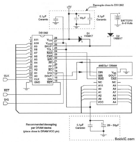
This circuit shows a DS1262 Serial DRAM nonvolatizer chip that is used to enable read/write access of DRAM from a simple 3-wire serial port. Refresh and RAS/CAS timing for the DRAM are performed automatically, transparent to operation of the serial port. In addition, the DS1262 performs all power switching and refresh duties that are necessary to retain DRAM data when the primary power supply fails. The backup supply input accepts a wide voltage range, suitable for use with rechargeable batteries. The DS1262 also provides an electronic gas gauge that can predict the condition of the backup supply. When the VCC1 power begins to drop, an internal circuit senses the changes, and the data-retention mode begins. The VCC1 input is then disconnected from the VCC0 output and the backup supply connected to the BKUP pin is switched in. The DS1262 also monitors the backup supply condition. If the backup supply is below VCC1, the backup-condition output pinBC is driven active low, and remains in this state until the backup supply voltage is restored to a level above VCC1. Dallas Semiconductors, Product Data Book, 1992/1993, p. 9-59. (View)
View full Circuit Diagram | Comments | Reading(1542)
TTL_DTL_interface_to_telephone_equipment
Published:2009/7/24 11:46:00 Author:Jessie
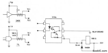
This circuit provides interface of positive-logic circuits to negative-powered telephone equipment. In addition, the circuit provides for a change in voltage level (+5 and -50 V), as well as isolation, using an H11G optoisolator. Motorola Thyristor Device Data, 1989, p. 6-54. (View)
View full Circuit Diagram | Comments | Reading(516)
A_MUX_with_16_bit_serial_interface
Published:2009/7/24 10:48:00 Author:Jessie
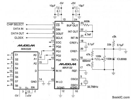
In this circuit, a 16-bit MAX132 A/D provides a serial interface for a MAX328 MUX, with both serial data input and output. The A/D is a 16-bit modified dual-slope converter. In addition to the main 16-bit output, the A/D also provides 3 guard-band bits with add resolution in the A/D noise region, but it can raise resolution if software averaging is used. The MAX328 MUX is addressed through four programmable bits PG0-PG3, which are sot through the MAX132 serial input. Maxim, 1992,Appications and Product Highlights, p. 8-4. (View)
View full Circuit Diagram | Comments | Reading(1601)
CLIPPING_POINT_INDICATOR
Published:2009/6/30 21:21:00 Author:May

Uses LED to indicate when clipping distortion begins in 50-W power amplifier. Display circuit is referenced to negative supply, making detection level Indopendent of supply variation; circuit thus works equally well for instantaneous, music, or continuous overloads. Tr1 is normally turned hard on and Tr2 is off. When overload makes collector-emitter voltage of lower amplifier output transistor approach saturation, Tr, begins to turn off and @, charges through D, so LED turns on. Attack time is chosen to make single 3-ms overload transient visible.-J. Dawson and K Northover, L.E.D. Clip Indicator, Wireless World, Jan. 1976, p 60. (View)
View full Circuit Diagram | Comments | Reading(1813)
DIVIDING_ANALOG_VOLTAGES
Published:2009/6/30 21:19:00 Author:May
Charge-and-dump V/F conversion technique is used to obtain quotient of two analog voltages digitally. Applications include measurement of total mass flow of gas under constant pressure. With Q1 and Q2 normally off, C1 charges at rate proportional to input E1, producing negative ramp at output of integrating opamp A1. When R2 wiper voltage exceeds E2, output of A2 goes high, tuming on Q3 and temporarily driving Q1 and Q2 into conduction. This process discharges C1, resetting output of A1 to zero. With values shown, E1 and E2 equal, and wiper of R2 at midpoint, circuit output is 10,000 pulses per hour, suitable for driving electromechanical counter. Output frequency is proportional to average DC value of E1 even when input changes rapidly.—H. L. Trietley, Voltage-to-Frequency Converter Performs Division, EDN Magazine, Jan. 5, 1978, p 79-80. (View)
View full Circuit Diagram | Comments | Reading(569)
TV_SOUND_IF_OR_FM_IF_AMPLIFIER_WITH_QUADRATURE_DETECTOR
Published:2009/6/30 21:18:00 Author:May
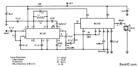
View full Circuit Diagram | Comments | Reading(1419)
IC_DflIVE_FOB_VU_METER
Published:2009/6/30 21:17:00 Author:May

Used in high-quality stereo cassette deck operating from AC line or battery. Meter rectifier bridge is in feedback loop of opamp, to give highly linear AC/DC conversion with flat frequency/amplitude response and short voltage rise time at low cost. Article gives all other circuits of cassette deck and describes operation in detaiL-J. L. Linsley Hood, Low-Noise, Low-Cost Cassette Deck, Wireless World, Part 1-May 1976, p 36-40 (Part 2-June 1976, p 62-66; Part 3-Aug. 1976, p 55-56). (View)
View full Circuit Diagram | Comments | Reading(869)
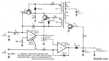
VOLTAGE_TO_PULSE_WIDTH
Published:2009/6/30 21:16:00 Author:May
Opamp and timer together convert input voltage level to width of output pulsewith accuracy better than 1%. Output is at same frequency as input.— Signetics Analog Data Manual, Signetics Sunnyvale, CA, 1977, p 726-727. (View)
View full Circuit Diagram | Comments | Reading(705)
VIDEO_IF_AMPLIFIER_AND_LOW_LEVEL_VIDEO_DETECTOR_CIRCUIT_1
Published:2009/6/30 21:16:00 Author:May

View full Circuit Diagram | Comments | Reading(530)
GRAY_TO_BINARY
Published:2009/6/30 21:15:00 Author:May

Convelts first 4 bits of Gray-code word to binary output. Uses two MC7496 shift registers and logic elements to transfer data serially from input register through MC1812 EXCLUSIVE-ORIC to output register. One requirement is that strobe on pin 8 of input register must complete its function before clock appears on pin 1 of register. When this and other timing conditions are satisfied, converter will work at speeds up to about 10 megabits per second.—J. Barnes, Analog-to-Digital Cyclic Converter, Motorola, Phoenix, AZ, 1974, AN-557, p 9. (View)
View full Circuit Diagram | Comments | Reading(2259)
TWO_STAGE_WIDEBAND_AMPLIFIER
Published:2009/6/30 21:15:00 Author:May
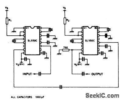
A wideband high gain configuration using two SL550s connected in series. The first stage is connected in common emitter config-uration, the second stage is a common base circuit. Stable gains of up to 65 dB can be achieved by the proper choice of R1 and R2. The bandwidth is 5 to 130 MHz, with a noise figure only marginally greater than the 2.0 dB specified for a single stage circuit. (View)
View full Circuit Diagram | Comments | Reading(617)
TELEVISION_IF_AMPLIFIER_AND_DETECTOR_USING_AN_MC1330_AND_AN_MC1352
Published:2009/6/30 21:14:00 Author:May

View full Circuit Diagram | Comments | Reading(871)
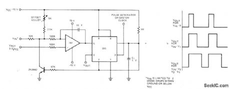
SINGLE_SLOPE_V_F_CONVERSlON
Published:2009/6/30 21:14:00 Author:May

UJT forms reference that determines reset point of LM301A integrator for converting analog input voltage to proportional frequency. Output of in-tegrator ramps negative until UJT switches and drives output positive at high slew rate. Positive edge of integ rator output is differentiated by RC network and level-shifted by NPN bipolar transistor to provide logic-compatible pulse.—J. Williams, Low-Cost, Linear A/D Conversion Uses Single-Slope Techniques, EDN Magazine, Aug. 5, 1978, p 101-104. (View)
View full Circuit Diagram | Comments | Reading(1284)
VIDEO_IF_AMPLIFIER_AND_LOW_LEVEL_VIDEO_DETECTOR_CIRCUIT
Published:2009/6/30 21:13:00 Author:May

The circuit has a typical voltage gain of 84 dB and a typical AGC range of 80 dB. It gives very small changes in bandpass shape, usually less than 1 dB tilt for 60 dB compression. There are no shielded sections. The detector uses a single tuned circuit (L3 and C10). Cou-pling between the two integrated circuits is achieved by a double tuned transformer (L1 and L2). (View)
View full Circuit Diagram | Comments | Reading(1048)
20_kHz_SQUARE_WAVE_TO_DC
Published:2009/6/30 21:13:00 Author:May

Provides accuracy within 0.1% for square-wave inputs of 3 to 7 VRMS in frequency range of 5 to 20 kHz when duty cycle is 50%. Opamps A1 and A2 are connected as differential input voltage-followers to provide high input impedance,A3 convolts to single-ended output as required by Model 440 convelter IC.A4 provides adjustable gain than roughly offsets attenuation of A3, with 2K pot being adiusted to provide desired ratio of DC output voltage to RMS value of input.—J. Renken, Differential High-Z RMS-DC Converter Has 0.1% Accuracy, EDN Magazine, May 5, 1977, p 114 and 116. (View)
View full Circuit Diagram | Comments | Reading(802)
001-10_V_to_110_OR_100_kHz
Published:2009/6/30 21:12:00 Author:May

Simple voltage-to-frequency converter uses Raytheon 4152 operating from single 15-V supply to convert analog input voltage to proportional frequency of square-wave output. Maximum output frequency depends on values used for resistors and capacitors, as given in table. Suitable for applications where input dynamic range is limited and does not go to zero.— Linear Integrated Circuit Data Book, Raytheon Semiconductor Division, Mountain View, CA, 1978, p 7-45-7-46. (View)
View full Circuit Diagram | Comments | Reading(834)
CURRENT_TO_VOLTAGE
Published:2009/6/30 21:12:00 Author:May

Developed for use with current-output transducers such as silicon photocells. For widest frequency response, circuit values may need some adjusting for source current and capacitance. C1, across feedback resistor of opamp, eliminates ringing around 500 kHz. If input coupling capacitor is added to reduce DC gain, circuit can be used with inductive source such as magnetic tape head.—R. S. Burwen, Current-to-Voltage Converter for Transducer Use, EDN Magazine, Dec. 15, 1972, p 40. (View)
View full Circuit Diagram | Comments | Reading(950)
| Pages:1216/2234 At 2012011202120312041205120612071208120912101211121212131214121512161217121812191220Under 20 |
Circuit Categories
power supply circuit
Amplifier Circuit
Basic Circuit
LED and Light Circuit
Sensor Circuit
Signal Processing
Electrical Equipment Circuit
Control Circuit
Remote Control Circuit
A/D-D/A Converter Circuit
Audio Circuit
Measuring and Test Circuit
Communication Circuit
Computer-Related Circuit
555 Circuit
Automotive Circuit
Repairing Circuit