
Circuit Diagram
Index 1218
SCHMITT_TRIGGER_WITH_PROGRAMMABLE_HYSTERESIS
Published:2009/6/30 3:44:00 Author:May
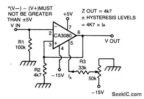
CA 3088 is used as a versatile Schmitt trigger. The size of the hysteresis levels is determined by IA that flows out of the amplifier's output and through R2. Increasing IA increases hysteresis and vice versa. The positive and negative hysteresis levels are symmetrical about 0 V. (View)
View full Circuit Diagram | Comments | Reading(803)
Basic_bipolar_output_DAC
Published:2009/7/24 9:41:00 Author:Jessie
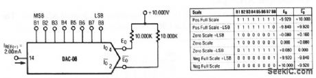
This circuit shows a DAC that is connected for bipolar-output D/A-converter operation. Raytheon Linear Integrated Circuits, 1989, p. 6-14. (View)
View full Circuit Diagram | Comments | Reading(0)
Basic_unipolar_negative_reference_DAC
Published:2009/7/24 9:41:00 Author:Jessie
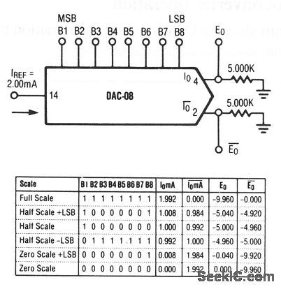
This circuit shows a DAC that is connected for unipolar negative-reference D/A-converter operation. Raytheon Linear Integrated Circuits, 1989, p. 6-13. (View)
View full Circuit Diagram | Comments | Reading(533)
Basic_positive_reference_DAC
Published:2009/7/24 9:40:00 Author:Jessie
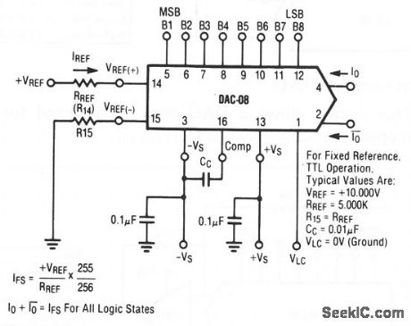
This circuit shows a DAC that is connected for D/A-converter operation. Raytheon Linear Integrated Circuits, 1989, p. 6-12. (View)
View full Circuit Diagram | Comments | Reading(773)
Three_input_AND_gate
Published:2009/7/24 9:39:00 Author:Jessie
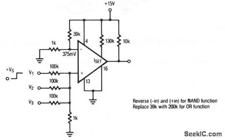
This circuit uses an LP165/365 comparator as a 3-input AND gate. The circuit can be converted to NAND or OR, as shown. Raytheon Linear Integrated Circuits, 1989, p. 5-43. (View)
View full Circuit Diagram | Comments | Reading(773)
TTL_to_MOS_logic_converter
Published:2009/7/24 9:37:00 Author:Jessie
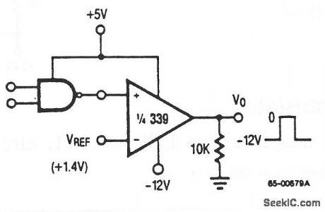
This circuit uses a 339 comparator to convert from TTL to MOS logic. Raytheon Linear Integrated Circuits, 1989, p. 5-31. (View)
View full Circuit Diagram | Comments | Reading(1580)
SCHMITT_TRIGGER_WITHOUT_HYSTERESIS
Published:2009/6/30 3:43:00 Author:May
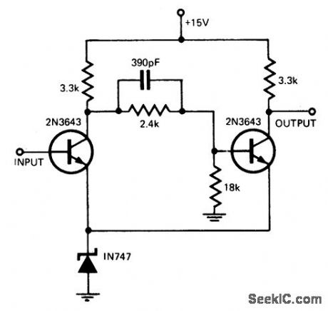
By replacing the common-emitter resistor in a conventional Schmitt by a zener diode, the hysteresis normally associated with these circuits is eliminated. (View)
View full Circuit Diagram | Comments | Reading(746)
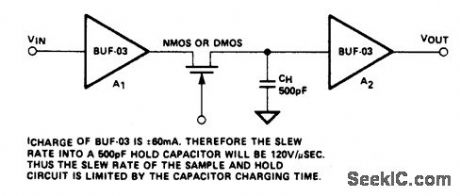
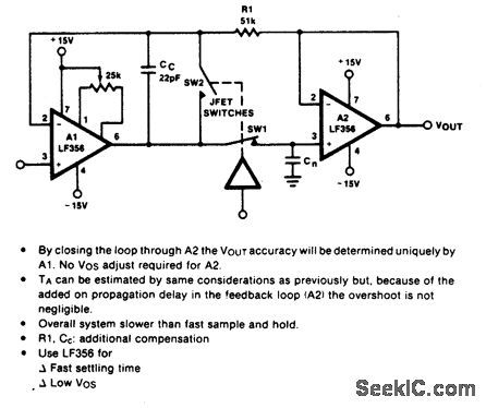
HIGH_SPEED_SAMPLE_AND_HOLD_2
Published:2009/6/30 3:41:00 Author:May
View full Circuit Diagram | Comments | Reading(432)
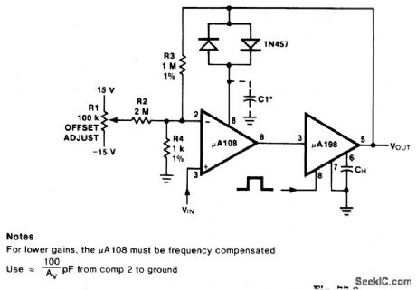
HIGH_ACCURACY_SAMPLE_AND_HOLD
Published:2009/6/30 3:39:00 Author:May
View full Circuit Diagram | Comments | Reading(507)
SAMPLE_AND_HOLD
Published:2009/6/30 3:39:00 Author:May
View full Circuit Diagram | Comments | Reading(1451)
×1000_SAMPLE_AND_HOLD
Published:2009/6/30 3:37:00 Author:May
(View)
View full Circuit Diagram | Comments | Reading(407)
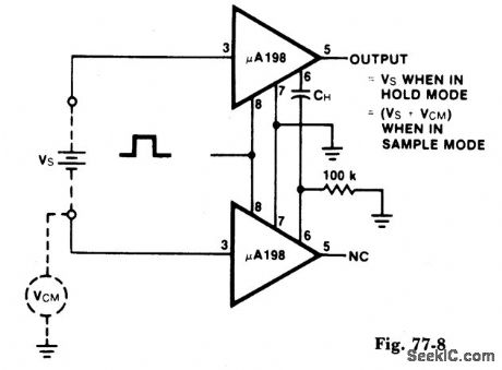
DIFFERENTIAL_HOLD
Published:2009/6/30 3:36:00 Author:May
View full Circuit Diagram | Comments | Reading(549)
EXCESS_THREE_GRAY_CODE_TO_BCD
Published:2009/6/30 3:36:00 Author:May
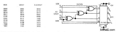
Develped for use with shaft encoder providing excess-three Gray-code output Requires only two TTL ICs, connected as shown. To convert regular Gray code to BCD, omit SN7483 4-bit adder.Tabulation shows how circuit accomplishes conversion for both types of Gray codes.—D. M. Risch, Two ICs Convert Excess-Three Gray Code to BCD, EDN Magazine, Nov. 1, 1972, p 44. (View)
View full Circuit Diagram | Comments | Reading(1702)
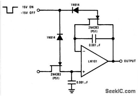
SAMPLE_AND_HOLD_WITH_OFFSET_ADJUSTMENT
Published:2009/6/30 3:35:00 Author:May
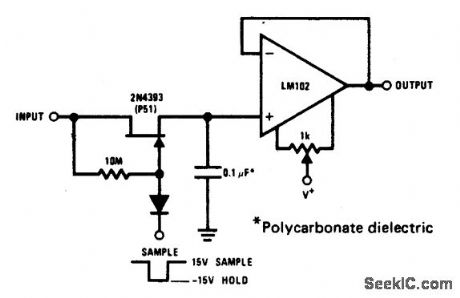
The 2N4393 JFET was selected because of its low IGss (<100 pA), very low ID(off) (< 100 pA) and low pinchoff voltage. Leakages of this level put the burden of circuit performance on clean, solder-resin free, low leakage circuit layout. (View)
View full Circuit Diagram | Comments | Reading(1336)
01_Hz_100_kHz_V_F
Published:2009/6/30 3:35:00 Author:May

Uses NE556 timer in dual mode in combination with opamp and FET for linear voltage-to-frequency conversion with output rangefrom 0.1 Hz to 100 kHz. Operatbg frequency is 0.91/2RC where R is resistance of FET.—K. Kraus, Linear V-F Converter, Wireless World, May 1977, p 80. (View)
View full Circuit Diagram | Comments | Reading(1970)
V_F_CONVERTER_WITH_005_LINEARITY
Published:2009/6/30 3:34:00 Author:May

Raytheon RM4151 converter is used with integrator opamp to give highly linear conversion of inputs up to -10 VDC to proportional frequency of square-wave output. With maximum input of -10 V, adjust 5K full-scale trimpot for maximum output frequency of 10 kHz. Set offset adjust pot to give 10-Hz output for input of -10 mV. To operate from single positive supply, change opamp to RC3403A.— Linear Integrated Circuit Data Book, Raytheon Semiconductor Division, Mountain View, CA, 1978, p 7-38. (View)
View full Circuit Diagram | Comments | Reading(958)
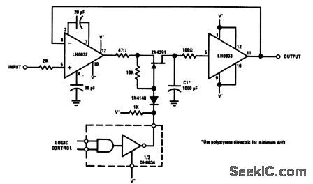
HIGH_SPEED_SAMPLE_AND_HOLD
Published:2009/6/30 3:31:00 Author:May
View full Circuit Diagram | Comments | Reading(1021)
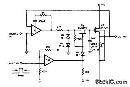
HIGH_SPEED_SAMPLE_AND_HOLD_1
Published:2009/6/30 3:33:00 Author:May
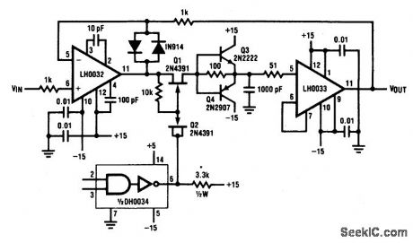
This circuit exhibits a 10 V acquisition time of 900 ns to 0.1% accuracy and a droop rate of only 100 μV/ms at 25°C ambient condition. An even faster acquisition time can be obtained using a smaller value hold-capacitor. By decreasing the value from 1000 pF to 220 pF, the acquisition time improves to 500 ns for a 10 V step. However, the droop rate increases to 500 μV/ms. (View)
View full Circuit Diagram | Comments | Reading(884)
10_Hz_TO_10_kHz_V_F
Published:2009/6/30 3:29:00 Author:May

External circuit shown for Teledyne 9400 Voltage-to-frequency converter provides means for trimming zero location and full-scale frequency value of output For 10-kHz full-scale value, set Vin to 10 mV and trim with 50K offset adjust pot to get 10-Hz output, then set V1, to 10.000 V and trim either Rin, VREF, or CREF to obtain 10-kHz output.—M. 0. Paiva, Applications of the 9400 Voltage to Frequency Frequency to Voltage Converter, Teledyne Semiconductor, Mountain View, CA, 1978, AN-10, p 3-5. (View)
View full Circuit Diagram | Comments | Reading(1227)
JFET_SAMPLE_AND_HOLD
Published:2009/6/30 3:24:00 Author:May
The logic voltage is applied simultaneously to the sample and hold JFETs. By matching input impedance and feedback resistance and capacitance, errors due to rds(on) of the JFETs are minimized. (View)
View full Circuit Diagram | Comments | Reading(860)
| Pages:1218/2234 At 2012011202120312041205120612071208120912101211121212131214121512161217121812191220Under 20 |
Circuit Categories
power supply circuit
Amplifier Circuit
Basic Circuit
LED and Light Circuit
Sensor Circuit
Signal Processing
Electrical Equipment Circuit
Control Circuit
Remote Control Circuit
A/D-D/A Converter Circuit
Audio Circuit
Measuring and Test Circuit
Communication Circuit
Computer-Related Circuit
555 Circuit
Automotive Circuit
Repairing Circuit