Basic Circuit
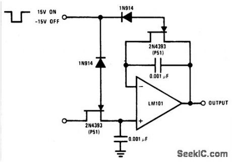
JFET_SAMPLE_AND_HOLD
Published:2009/6/30 3:24:00 Author:May | From:SeekIC

The logic voltage is applied simultaneously to the sample and hold JFETs. By matching input impedance and feedback resistance and capacitance, errors due to rds(on) of the JFETs are minimized.
Reprinted Url Of This Article:
http://www.seekic.com/circuit_diagram/Basic_Circuit/JFET_SAMPLE_AND_HOLD.html
Print this Page | Comments | Reading(3)

Article Categories
power supply circuit
Amplifier Circuit
Basic Circuit
LED and Light Circuit
Sensor Circuit
Signal Processing
Electrical Equipment Circuit
Control Circuit
Remote Control Circuit
A/D-D/A Converter Circuit
Audio Circuit
Measuring and Test Circuit
Communication Circuit
Computer-Related Circuit
555 Circuit
Automotive Circuit
Repairing Circuit
Code: