
Circuit Diagram
Index 1207
RAIN_WARNING_BLEEPER
Published:2009/7/1 0:37:00 Author:May
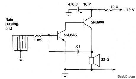
One small spot of rain on the sense pad of this bleeper will start this audio warning.It can also be operated by rising water. The circuit has two transistors, with feedback via capacitor C1, but Trl cannot operate as long as the moisture sense pad is dry. When the pad conducts, Tr1 and Tr2 form an audio oscillatory circuit, the pitch depends somewhat on the resistance. (View)
View full Circuit Diagram | Comments | Reading(759)
GAS_AND_VAPOR_DETECTOR
Published:2009/7/1 0:34:00 Author:May
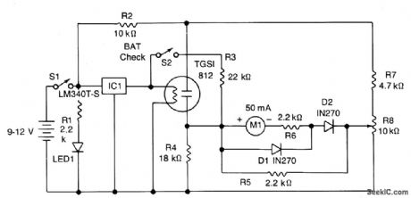
The power drain is approximately 150 mA. IC1 provides a regulated 5-volt supply for the filament heater of the sensor. The gas sensitive element is connected as one arm of a resistance bridge consisting of R4, R7, R8 and the meter Ml with its associated resistors R5 and R6. The bridge can be balanced by adjusting R8 so that no current flows through the meter. A change in the sensor's resistance, caused by detection of noxious gases, will unbalance the circuit and deflect the meter. Diodes D1, D2 and resistor R5 protect the meter from overload while R6 determines overall sensitivity. R2 limits the current through the sensor; R1 and LED1 indicate that the circuit is working, so that you do not drain the battery leaving the unit on inadvertently; R3 and S2 give a battery level check. (View)
View full Circuit Diagram | Comments | Reading(727)
AIR_FLOW_DETECTOR
Published:2009/7/1 0:34:00 Author:May

View full Circuit Diagram | Comments | Reading(0)
LIE_DETECTOR
Published:2009/7/1 0:33:00 Author:May
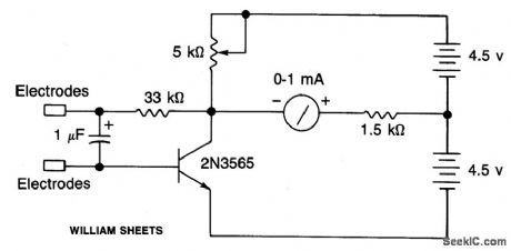
The two probes shown are held in the hands and the skin resistance applies bias to the transistor. The 5 k ohm pot is set for zero deflection on the meter. When the subject is embarrassed or lies, sweating on the hands takes place, increasing the bias to the transistor and upsetting the bridge balance. (View)
View full Circuit Diagram | Comments | Reading(1839)
Crystal_stabilized_relaxation_oscillator
Published:2009/7/24 7:50:00 Author:Jessie
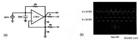
This circuit shows an LT1011 connected as a simple relaxation oscillator with crystal control. Figure 5-28B shows the corresponding waveforms. Waveform A is taken from the inverting ( -) input of the LT1011, while waveform B is taken from the LT1011 output. Linear Technology Corporation. Linear Appications Handbook, 1990, p. AN12-3, -2. (View)
View full Circuit Diagram | Comments | Reading(717)
ELECTRONIC_ROULETTE
Published:2009/7/1 0:32:00 Author:May

U1 (a 4046 PLL containing a voltage controlled oscillator or VCO, two phase comparators, a source follower, and a Zener diode) is used to produce a low-frequency, pulsed output of about 40 Hz. The VCO's frequency range is determined by R6 and C2, which can. be altered by varying the voltage at pin 9. The rising voltage causes the frequency to rise from zero to threshold and remain at that frequency as long as 51 is closed. When S1 is opened, C1 discharges slowly through RI to ground and the voltage falls toward zero. That produces a decreasing pulse rate. The output of UI at pin 4 is connected to the clock input of U2 (a 4017 decade decoder/driver) at pin 14 via C3. U2 sequentially advances through each of its ten outputs (0 to 9)-pins 1 to 7, and 9 to 11-with each input pulse. As each output goes high, its associated LED is lighted, and extinguished when it returns to the low state. Only eight outputs are used in the circuit, giving two numbers to the spinner of the house. The circuit can be set up so that the LED's lights sequence or you can use some staggered combination; the LEDs grouped in a straight line or a circle. (View)
View full Circuit Diagram | Comments | Reading(1461)
Simple_clock_oscillators
Published:2009/7/24 7:48:00 Author:Jessie
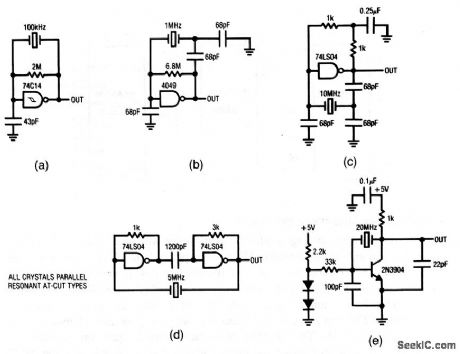
These circuits show four basic clock oscillators composed of digital IC gates, and a discrete-component oscillator, all of which are well suited as clock sources. Notice that the diodes used in the discrete-component oscillator can be 1N4148s or equivalent. Linear Technology Corporation, Linear Applications Handbook, 1990, p. AN12-2. (View)
View full Circuit Diagram | Comments | Reading(1177)
THERMALLY_BASED_ANEMOMETER(AIR_FLOWMETER)
Published:2009/7/1 0:32:00 Author:May


This design used to measure air or gas flow works by measunng the energy required to maintain a heated resistance wlre at constant temperature. The positive temperature coefficient of a small lamp,in combination with its ready availability,makes it a goodsensor,A type 328 lamp is modified for this circuit by removlng its glass envelope,Thelamp IS placed h a bridge whichis monitored by A1. A1's output iS current amplifiedby Q1 and fed back to drive the bridge,When power IS applied,the lamp IS at a lowresistance and Q1's emitter tries to come fun on.As current flows through the lamp,its temperature quickly rises,forcing its resistance to increase.This action increasesA1's negative input potential.Q1's emltter voltage decreases and the circuit finds a stableoperating point.To keep the bridge balanced,A1 acts to force the lamp's resistance,hence its temperature,constant,The 20 k - 2 k bridge values have been chosen so that the lamp operates just below the incandescence point.To use this circuit,place the lamp in the air flow so that its filament is at a 90°angle to the flow.Next,either shut off the air flow or shield the lamp from it and adjust the zero flow potentiometer for a circuit output of 0 V.Then,expose the lamp to air flow of 1000 feet/minute and trim the full flow potentiometer for 10 Ⅴ output.Repeat these adjustments until both points are fixed.With this procedure completed,the air flowmeter iS accurate within 3%over the entire 0-1000 foot/minute range.
(View)
View full Circuit Diagram | Comments | Reading(1473)
High_purity_sine_wave_generator
Published:2009/7/24 7:46:00 Author:Jessie

By combining a MAX270 4th-order low-pass filter, a 74HC163 counter, and an 8-channel analog MUX, high-purity 1- to 25-kHz sine waves are generated with a THD of less than -80 dB. The low-pass filter is set to the desired frequency and a clock 8 times the sine frequency is applied to the 74HC163 counter. The MAX270 uncommitted op amp sets the filter output level. Gain accuracy is set by the MAC270 gain at the corner frequency, which is guaranteed between -2.4 and -3.6 dB at 1 kHz. The 100-kΩ potentiometer provides gain control if desired. Two resistor dividers provide the input voltages that are required at the MUX inputs. When the MUX switches through channels 0 to 7, an 8-times oversampled staircase approximation of a sine wave is generated. Compared with a square wave, the oversampled waveform greatly reduces smoothing-filter requirements by pushing the first significant harmonic out to 7 times the fundamental. All higher-order harmonics are filtered to below -80 dB by the MAX270. Maxim , 1992, Applications and Product Highlights, p. 7-7. (View)
View full Circuit Diagram | Comments | Reading(1700)
15_V_powered_temperature_compensated_crystal_oscillator
Published:2009/7/24 7:44:00 Author:Jessie
This fully temperature-compensated oscillator is operated from a 1.5-V source (single battery) and draws only 230-μA current, making the circuit ideal for portable high-accuracy clocks, survival radios, and secure communications. Linear Technology Corporation, 1991, AN45-14. (View)
View full Circuit Diagram | Comments | Reading(598)
TRIANGLE_TO_SINE_CONVERTERS
Published:2009/7/1 0:01:00 Author:May

Conversion of triangle wave shapes to sinusoids is usually accomplished by diode-resistor shaping networks, which accurately reconstruct the sine wave segment by segment. Two simpler and less costly methods may be used to shape the triangle waveform of the 566 into a sinusoid with less than 2% distortion. The non-linear IDSVDS transfer characteristic of a P-channel junction FET is used to shape the triangle waveform.The amplitude of the triangle waveform is critical and must be carefully adjusted to achieve a low distortion sinusoidal output. Naturally, where additional waveform accuracy is needed, the diode-resistor shaping scheme can be applied to the 566 with excellent results since it has very good output amplitude stability when operated from a regulated supply. (View)
View full Circuit Diagram | Comments | Reading(2819)
Quartz_stabilized_4_kHz_oscillator_with_9_ppm_distortion
Published:2009/7/24 7:40:00 Author:Jessie

A spectrally pure sine-wave oscillator is required for data converter, filter, and audio testing. This oscillator has less than 9 ppm (0.0009%) distortion in the 10-Vpp output. The circuit is adjusted for minimum distortion by adjusting the 50-kΩ potentiometer while monitoring the A3 output with a distortion analyzer. This trim sets the voltage across the photocell to the optimum value for lowest distortion. Linear Technology Corporation, 1991, AN45-12. (View)
View full Circuit Diagram | Comments | Reading(715)
LIGHT_SEEKING_ROBOT
Published:2009/6/30 23:58:00 Author:May

The circuit is light seeking; it will follow a flashlight around a darkened room. A pair of photocells determine the direction in which the robot will move. Each photocell is connected to an op amp configured as a comparator. When sufficient light falls on photocell R2, the voltage at the inverting input (pin 6) of ICl-a will fall below the voltage at the non-inverting input (pin 5), so the output of the comparator will go high, and transistors Q1 and Q2 will turn on. That will enable relays RY1 and RY2, and thereby provide power for the right motor. The robot will then turn left. Likewise, when light falling on R3 lowers its resistance, Q2 and Q3 will turn on, the left motor will energize, and the robot will turn right. (View)
View full Circuit Diagram | Comments | Reading(3003)
CURRENT_TO_VOLTAGE_CONVERTER_WITH_GROUNDED_BIAS_AND_SENSOR
Published:2009/6/30 23:58:00 Author:May

View full Circuit Diagram | Comments | Reading(1735)
Floating_current_loop_transmitter
Published:2009/7/24 7:38:00 Author:Jessie

A 4- to 20-mA current-loop transmitter is frequently required in industrial process control. Because of uncertain or dangerous common-mode voltages, it is desirable that the generated current be completely galvanically isolated from the transmitter input. This circuit does this while operating from a single 5-V supply. To calibrate this circuit, apply 0-V input and adjust the 4-mA trim for 4.00-mA output (0.064 V across the 16-Ω shunt). Next, apply 2.56-V input and set the 20-mA trim for 20.00-mA output (0.3200 V across the 16-Ω shunt). Repeat this procedure until both points are fixed. Notice that the 2.56-V input range is directly compatible with D/A converter (chapter 6) outputs, which permits digital control. Linear Technology Corporation, 1991, AN45-6. (View)
View full Circuit Diagram | Comments | Reading(823)
PHOTODIODE_SENSOR_AMPLIFIER
Published:2009/6/30 23:57:00 Author:May

View full Circuit Diagram | Comments | Reading(1090)
Trigger_with_adaptive_threshold
Published:2009/7/24 7:33:00 Author:Jessie

This circuit triggers from dc to 50 MHz over a 2- to 300-mV input range with no level adjustment. The circuit maintains the A3 output trip-point at one-half the input amplitude, regardless of input magnitude. This ensures reliable automatic triggering over a wide input amplitude range-even for very low-level inputs. As an option, the network shown in dashed lines permits changing the trip threshold. This allows any point on the input waveform edge to be selected as the trigger point. Figure 5-22B shows performance for a 40-MHz input sine wave (Trace A). The A1 output (Trace B) takes gain and the A3 output (Trace C) produces a clean 5-V signal. Linear Technology Corporation, 1991, AN47-59. (View)
View full Circuit Diagram | Comments | Reading(880)
LED_FLASHER_USES_PUT
Published:2009/6/30 23:57:00 Author:May


This flasher circuit operates as a relaxation oscillator with C1 discharged periodically through the LED as the PUT as the the put switches on. the flashing rate is about 100/minute with the component values listed. (View)
View full Circuit Diagram | Comments | Reading(1057)
ELECTRONIC_WAKE_UP_CALL
Published:2009/6/30 23:57:00 Author:May

A cadmium sulfide photocell (LDR1, which is a light-dependent resistor) is connected to the base and collector of an npn transistor, Q1. When light hits LDR1, the internal resistance goes from a very high (dark) value to a low (light) value, supplying base current to Q1, turning it on. The voltage across RI produces a bias that turns Q2 on, which in turn, supplies the positive voltage to U1 at pin 8 (the positive-supply input) and pin 4 (the reset input), to operate the 555 audio oscillator circuit. The circuit's sensitivity to light can be set via R6 (a 50,000 ohm potentiometer). R7 sets the audio tone to the most desirable sound. The squarewave audio tone is fed from U1 pin 3 to a small speaker through coupling capacitor C4 and current limiting resistor R4. (View)
View full Circuit Diagram | Comments | Reading(809)
CAPACITANCE_TO_PULSE_WIDTH_CONVERTER
Published:2009/6/30 23:57:00 Author:May

View full Circuit Diagram | Comments | Reading(849)
| Pages:1207/2234 At 2012011202120312041205120612071208120912101211121212131214121512161217121812191220Under 20 |
Circuit Categories
power supply circuit
Amplifier Circuit
Basic Circuit
LED and Light Circuit
Sensor Circuit
Signal Processing
Electrical Equipment Circuit
Control Circuit
Remote Control Circuit
A/D-D/A Converter Circuit
Audio Circuit
Measuring and Test Circuit
Communication Circuit
Computer-Related Circuit
555 Circuit
Automotive Circuit
Repairing Circuit