
Circuit Diagram
Index 1208
Avalanche_pulse_generator_for_rise_fall_measurements
Published:2009/7/24 7:27:00 Author:Jessie


This circuit draws only about 5 mA from the 1.5-V battery, and produces a 10-V pulse with a typical rise and fall time of about 350 ps. Q1 might require selection to get the desired avalanche behavior. A sample of 50 Motorola 2N2369s, spread over a 12-year date-code span,yielded 82%(with some in the 220- to 230-ps range). All good 2N2369s switched in less than 650 ps. C1 is selected for a 10-V amplitude output. The value spread is typically 2 to 4 pF. Ground-plane construction with high-speed layout techniques are essential for good results from this circuit. Linear Technology Corporations 1991, AN47-93. (View)
View full Circuit Diagram | Comments | Reading(1666)
Varactor_tuned_Wien_bridge_oscillator
Published:2009/7/24 7:26:00 Author:Jessie
This circuit replaces the lamp (Fig. 5-18) and electronic control (Fig. 5-19) with a Wien network to produce a variable-frequency output from 1 to 10 MHz. Usually, Wien circuits require manually adjustable elements (dual pots or two-section variable capacitors) for tuning. In this circuit, the Wien-network resistors are fixed (360Ω), and the capacitive elements are accomplished with varactor diodes. The circuit is tuned by a control voltage at the noninverting input of A3. Figure 5-20B is a spectrum analysis of the oscillator output. Linear Technology corporation, 1991, AN47-51. (View)
View full Circuit Diagram | Comments | Reading(938)
Quartz_stabilized_oscillator_with_electronic_gain_control
Published:2009/7/24 7:21:00 Author:Jessie


This circuit replaces the lamp(Fig. 5-18)with an electronic gain control or stabilization loop. To use this circuit, adjust the 50-Ω trimmer until 2-Vpp oscillations appear at the output of A1. Figure 5-19B is a spectrum analysis of the oscillator output. Linear Technology Corporation, 1991, AN47-50. (View)
View full Circuit Diagram | Comments | Reading(637)
AUTOMATIC_MOORING_LIGHT
Published:2009/6/30 23:55:00 Author:May

Integrated-circuit U1-an LF351 or 741 op amp-is used as a comparator to control the light. Resistors R2 and R3 provide a reference voltage of about 2.5 volts at pin 3 of U1. When daylight falls on light-dependent resistor LDR1, its resistance is low: about 1000 ohms. In darkness, the LDR's resistance rises to about 1 megohm. Since R1 is 100,000 ohms, and the LDR in daylight is 1000 ohms, the voltage ratio is 100 to 1; the voltage drop across the LDR is less than the 2.5 volt reference voltage and pin 2 of U1 is held at that voltage. In that state, the output at pin 6 of U1 is positive at about 4.5 volts, a value that reverse-biases Q1 to cutoff, which in turn holds Q2 in cutoff, thereby keeping lamp I1 off. When darkness falls, the LDR's resistance rises above R1's value and the voltage at pin 2 of U1 rises above the reference voltage of 2.5 volts. U1's output terminal (pin 6) falls to less than a volt and Q1 is biased on. The base-to-emitter current flow turns Q2 on, which causes current to flow through the lamp. When daylight arrives, the LDR's resistance falls sharply, which causes the lamp to be turned off, ready to repeat the next night/day cycle. (View)
View full Circuit Diagram | Comments | Reading(898)
GAS_DISCHARGE_DISPLA
Published:2009/6/30 23:55:00 Author:May


National MM5309 digital clock glves choice of 12-or 24-h displayand 50-or 60-Hz operation for drving 4-digit gas-discharge display having colon and AM/PM indications. Separate cathode driver and sepa-rate anode driver are required for each digit.- MOS/LSI Databook, National Demiconductor, Santa Clara,CA,1977,p 1-2-1-8 (View)
View full Circuit Diagram | Comments | Reading(1660)
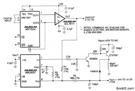
A_REGULATED_DC_TO_DC_CONVERTER
Published:2009/6/30 23:55:00 Author:May

View full Circuit Diagram | Comments | Reading(852)
Basic_quartz_stabilized_oscillator
Published:2009/7/24 7:17:00 Author:Jessie

This circuit uses a crystal within an amplifier's feedback path to create an oscillator. Although shown as 10 MHz, the circuit works well with a wide variety of crystal types over a 100-kHz to 20-MHz range. The use of a lamp to control amplifier gain is a classic technique that was first used in 1938. Linear Technology Corporation, 1991, AN47-49. (View)
View full Circuit Diagram | Comments | Reading(598)
TWILIGHT_TRIGGERED_CIRCUIT
Published:2009/6/30 23:53:00 Author:May
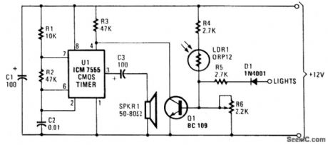
As dusk begins to fall, the sensor (a cadmium-sulftde light-dependent resistor or LDR) operates a small horn to provide an audible reminder that it's time to turn on your lights. To turn the circuit off-simply turn your headlights on and the noise stops. The base of Q1 is fed through a voltage divider formed by R4, LDRl-a light-dependent resistor with an internal resistor of about 100 ohms under bright-light conditions and about 10 megohms in total darkness-potentiometer R6. Q1's base voltage depends on the light level received by LDR1 and the setting of R6. If LDR1 detects a high light level, its resistance decreases, thereby providing a greater base current for Q1, causing it to conduct. When Q1 conducts, pin 4 of UI is pulled to near ground potential, muting the oscillator. If; on the other hand, LDR1 detects a low light level, its resistance increases (reducing base currentto Q1), cutting off the transistor and enabling the oscillator. In actual practice, you set R6 so that at a suitable light level (dusk), the oscillator will sound.The anode of diode Dl connects to the light switch, where it connects to the vehicle's parking lights. With the lights switched off, that point is connected to the negative chassis by way of the parking lamp. That has no effect on the circuit, as Dl blocks any current flow to ground from Q1's base via R6 and the sidelight lamps. When the lights are switched on, the anode of Dl is connected to the positive supply via the parking lamp switch, thereby applying a voltage to the base of Q1, biasing it into conduction. With Q1 conducting, pin 4 of UI is pulled virtually to ground, disabling the oscillator even though LDRl's resistance is not enough to do so. (View)
View full Circuit Diagram | Comments | Reading(927)
Regenerative_sine_wave_converter
Published:2009/7/24 7:16:00 Author:Jessie

This circuit uses an XR-2211 PLL and an XR-2208 multiplier to form a universal sine-wave converter. The circuit converts any periodic input-signal waveform to a low-distortion sine-wave, the frequency of which is identical to the repetition rate of the input signal. The center frequency, fO, is determined by the values of CO and RO. With RO at 10 kΩ, as shown, the value of CO is determined by: CO(inμF)=100/fO in Hz. Notice that the XR-2211 VCO might not oscillate if RO is greater than 10 kΩ. The distortion and amplitude of the sine-wave output is adjusted by RX, and RF, as shown. EXAR Corporation Databook, 1990, p. 5-312. (View)
View full Circuit Diagram | Comments | Reading(3250)
TTL_SQUARE_WAVE_TO_TRIANGLE_CONVERTER
Published:2009/6/30 23:53:00 Author:May

This fixed frequency triangular waveform generator driven by a TTL square wave generates typically 16-V p-p triangles at frequencies up to several MHz. It uses only one NAND open collector gate, or one open collector inverter as a fast integrator with gain.Careful successive adjustments of R and P1 are needed. When correct adjustments are reached, output amplitude and linearity are largely independent of the value of VB, from a minimum of 18 V up to 35 V. The value of C shown is for 100 kHz; at higher frequencies, it must be reduced in proportion. (View)
View full Circuit Diagram | Comments | Reading(2344)
BACK_BIASED_GaAsP_LED_OPERATES_AS_LIGHT_SENSOR
Published:2009/6/30 23:52:00 Author:May

Using a simple 741 amplifier connected as a current-to-voltage converter with the LED as the current source, the voltage at the output is proportional to incident light. The junction is biased only by the difference between the summing node junction potential and ground, preventing the possibility of reverse break-down. The photon-generated current equals the short-circuit current of the junction, which is linearly related to incident light. The sensor requires a level of incident illumination that depends on the degree of opacity of the LED package. (View)
View full Circuit Diagram | Comments | Reading(3077)
PHOTOELECTRIC_SWITCH
Published:2009/6/30 23:51:00 Author:May

The CDS cell resistance decreases in the presence of light, turning on the 2N3904 relay driver. (View)
View full Circuit Diagram | Comments | Reading(3395)
TTL_TO_MOS_LOGIC_CONVERTER
Published:2009/6/30 23:51:00 Author:May

View full Circuit Diagram | Comments | Reading(0)
Digital_power_monitor_with_early_warning
Published:2009/7/24 12:21:00 Author:Jessie
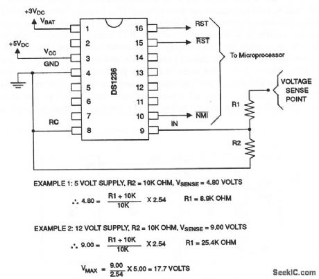
This circuit shows a DS1236 that is used to control a digital-system power supply. The DS1236 generates a nonmaskable interrupt (NMI ) for early warning of power failure to a microprocessor. A precision comparator monitors the voltage level at the In pin, relative to an internal reference. The In pin is a high-impedance input that allows for a user-defined sense point. An external resistor voltage divider interfaces with voltage signals. The sense point can be taken from the 5-V supply or from a higher voltage level that is closer to the main system power input. Because the In trip point VTP is 2.54 V,the proper values for R1 and R2 can be determined by the equations. Dallas Semiconductors, Product Data Book, 1992/1993, p. 7-74. (View)
View full Circuit Diagram | Comments | Reading(522)
Digital_signal_processing_system_with_anti_aliasing
Published:2009/7/24 10:46:00 Author:Jessie
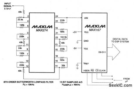
In this circuit, a MAX274 provides a front-end 10-kHz low-pass filter to a digital signal-processing (DSP) system. Signals between dc and 10 kHz are digitized by a 12-bit sampling MAX167 A/D. The DSP processor receives samples at a rate of 48 kHz. The input signal is filtered by a MAX274 that is configured as a 10-kHz 8th-order Butterworth low-pass filter. Signals above 24 kHz (the Nyquist frequency) are attenuated 60 dB. Additional rolloff in the incoming signal reduces potential alias frequencies below the theoretical 74-dB noise floor of the 12-bit system. Maxim, 1992, Applications and Product Highlights, p. 7-4. (View)
View full Circuit Diagram | Comments | Reading(1110)
Flash_EPROM_programmer_plus_adjustable_LCD_supply
Published:2009/7/24 10:43:00 Author:Jessie
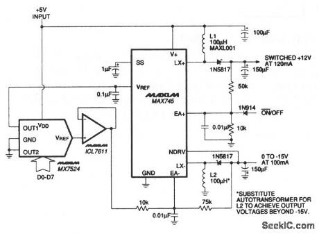
The MAX745 generates both positive and negative boosted outputs from a +5-V supply. This circuit is configured for small microprocessor systems, and contains a DAC to adjust the negative voltage for LCD contrast control. The circuit also provides for switching on and off the + 12-V output to program flash EPROMs. Maxim, 1992, Applications and Product Highlights, p. 4-9. (View)
View full Circuit Diagram | Comments | Reading(947)
Flash_EPROM_programmer
Published:2009/7/24 10:39:00 Author:Jessie

The MAX732 current-mode PWM regulator makes a good flash EPROM programmer because of the logic-compatible shutdown control, and because the supply is capable of programming four flash devices simultaneously. When heavily loaded, the MAX732 operates in the continuous-conduction mode, where inductor current never returns to zero. When inductor current is depleted, the LX voltage rings around the level of the input supply voltage. This is caused by the tank circuit, which is formed by the inductor and stray capacitances (windings, diode, MOSFET within the chip, etc.). Maxim, 1992, Applications and Product Highlights, p. 4-7. (View)
View full Circuit Diagram | Comments | Reading(1576)
LIGHT_OPERATED_SWITCH
Published:2009/6/30 23:50:00 Author:May

This circuit uses a flip-flop arrangement of Q1 and Q2. Normally Q1 is conducting heavily. Light on CDS photocell causes Q1 bias to decrease, cutting it off, tuming on Q2, removing the remaining bias from Q1. Reset is accomplished by depressing S1. (View)
View full Circuit Diagram | Comments | Reading(689)
LCD_supply_with_digital_adjust
Published:2009/7/24 10:35:00 Author:Jessie
If the expense of a customized autotransformer (L1, Fig. 6-25) is too high, this low-cost pulse-skipping circuit can be used. In this case, the relatively high output voltage is accommodated via an extemal switch transistor that has 40-V BVCEO specifications. A simple D/A scheme adjusts the output for contrast control and temperature compensation of the LCD. Maxim, 1992, Applications and Product Highlights, p. 4-5. (View)
View full Circuit Diagram | Comments | Reading(627)
WARNING_LIGHT_OPERATES_FROM_BATTERY_POWER_SUPPLY
Published:2009/6/30 23:50:00 Author:May

The circuit provides illumination when darkness comes. By using the gain available in darlington transistors, this circuit is simplified to use just a photodarlington sensor, a darlington amplifier, and three resistors. The illumination level will be slightly lower than normal, and longer bulb life can be expected, since the D40K saturation voltage lowers the lamp operating voltage slightly. (View)
View full Circuit Diagram | Comments | Reading(929)
| Pages:1208/2234 At 2012011202120312041205120612071208120912101211121212131214121512161217121812191220Under 20 |
Circuit Categories
power supply circuit
Amplifier Circuit
Basic Circuit
LED and Light Circuit
Sensor Circuit
Signal Processing
Electrical Equipment Circuit
Control Circuit
Remote Control Circuit
A/D-D/A Converter Circuit
Audio Circuit
Measuring and Test Circuit
Communication Circuit
Computer-Related Circuit
555 Circuit
Automotive Circuit
Repairing Circuit