
Circuit Diagram
Index 1213
POSITIVE_PEAK_DETECTOR
Published:2009/6/30 22:24:00 Author:May


CA3100 bipolar MOS opamp is connected as wideband noninverting amplifierto provide essentiany constantgain for wide range of input frequendes,Diode clips negative half-cycles, so output of transistor is proportional only to positive input peaks.- Circuit Ideas for RCA Linear ICs, RCA Solid State Division, Somerville, NJ, 1977, p 16. (View)
View full Circuit Diagram | Comments | Reading(0)
WIDEBAND_AGC_AMPLIFIER
Published:2009/6/30 22:23:00 Author:May

Combination of 592K opamp and MC1496K balanced modulator gives DC output signal proportional to amplitude of AC input signal, for varying gain of balanced modulator. Unbalancing carrier input of modulator makes signal pass through without attenuation.- Sig netics Analog Data Man-ual, Signetics, Sunnyvale, CA, 1977, p 709-710. (View)
View full Circuit Diagram | Comments | Reading(1076)
AGC_LOOP_FOR_MOSFETS
Published:2009/6/30 22:22:00 Author:May

Used at output of 9-MHz IF amplifier in commercial receiver to divide desired control-voltage magnitude and swing for FT0601 MOSFETS in IF strip. MOSFETs are biased by 2.1,V zeners in source leads in FETs, to drive gate-2 voltage sufficiently nega-tive for full AGC action.-G. Ricaud, Modifying the W1CER/W1FB AGC Loop for Usewith M0S-FET I-F Amplifiers, OST, June 1977, p 47 (View)
View full Circuit Diagram | Comments | Reading(2017)
CONTROL_AT_LOW_GAIN_LEVELS
Published:2009/6/30 22:22:00 Author:May

Diode is used as variable impedance in voltage-divider network at input of video amplifier to provide AGC at lower gain levels than could be handled with more conventional external-diode circuits. Voltage gain for Motorola MC1552 decreases from about 50 for 1-mA AGO control current to about 20 for 8 mA. For MC1553 high-gain video amplifier, gain drops from 400 at 1 mA to 25 at 8 mA.- A Wide Band Monolithic Video Amplifier, Motorola, Phoenix,AZ, 1973, AN-404 p 11. (View)
View full Circuit Diagram | Comments | Reading(728)
CONTROL_WITH_EXTERNAL_DIODE
Published:2009/6/30 22:21:00 Author:May
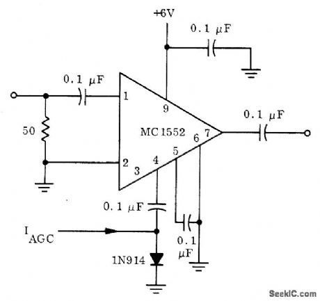
External resistances normally used with Motorola MC1552 video amplifier are replaced by 1N914 or equivalent diode so gain of amplifier is de-termined by AGO current through diode. Arrangement gives wide range of gain control, but lowest obtainable level of gain is normal unmodified gain off amplifier. Same circuit can be used with MC1553 highgain video amplifier.- A Wide Band Monolithic Video Amplifier, Motorola, Phoenix, M, 1973, AN-404 p 10. (View)
View full Circuit Diagram | Comments | Reading(504)
HIGH_SPEED_SAMPLE_AND_HOLD_AMPLIFIER
Published:2009/6/30 3:29:00 Author:May

View full Circuit Diagram | Comments | Reading(494)
TTL_driver
Published:2009/7/24 9:35:00 Author:Jessie
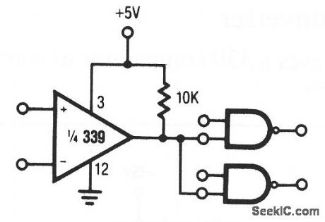
This circuit uses a 339 comparator as a TTL driver. Raytheon Linear Integrated Circuits, 1989, p. 5-30. (View)
View full Circuit Diagram | Comments | Reading(743)
One_shot_multivibrator
Published:2009/7/24 9:09:00 Author:Jessie

This circuit uses two LM3900 Norton amplifiers as a one-shot or monostable MV. CR1 can be a 1N914 or equivalent. National Semiconductor, Linear Applications Handbook, 1991, p. 242. (View)
View full Circuit Diagram | Comments | Reading(0)
Complementary_trigger_flip_flop
Published:2009/7/24 9:08:00 Author:Jessie

This circuit uses two LM3900 Norton amplifiers as a complementary flip-flop or as a divide-by-two configuration. National Semiconductor, Linear Applications Handbook, 1991, p. 241. (View)
View full Circuit Diagram | Comments | Reading(756)
5_V_to_isolated_5_V_at_20_mA
Published:2009/7/24 9:08:00 Author:Jessie

In this circuit, a negative-output dc/dc converter generates a -5-V output at point A. To generate this -5 V at A, the transformer primary must flyback to a diode drop that is more negative than -5 V. If the transformer has a tightly-coupled 1:1 turns ratio, 5 V (plus a diode drop) is across the secondary. The 1N5817 rectifies this secondary voltage to generate an isolated 5-V output (which is not fully regulated because the -5 V at point A is sensed by the MAX635). With careful transformer selection, the 5-V output will be within 10%. Bifilar winding of the transformer provides better load regulation of the isolated 5-V output, but this does reduce the isolation by increasing the capacitance between the primary and secondary. The isolation voltage breakdown is determined by the characteristics of the transformer, not the MAX635. (View)
View full Circuit Diagram | Comments | Reading(582)
Trigger_flip_flop
Published:2009/7/24 9:07:00 Author:Jessie

This circuit uses an LM3900 Norton amplifier as a trigger flip-flop as a divide-by-two configuration. CR1 and CR2 can be 1N914s or equivalent. National Semiconductor, Linear Applications Handbook, 1991, p. 241. (View)
View full Circuit Diagram | Comments | Reading(1427)
Isolated__15_V_dc_dc_converter
Published:2009/7/24 9:07:00 Author:Jessie

In this circuit, a TL431 shunt regulator is used to sense the output voltage. The TL431 drives the LED of a 4N28 optocoupler, which provides feedback to the MAX641 while maintaining isolation between the + 12-V input and the +15-V output (which is fully regulated with respect to both line and load changes). (View)
View full Circuit Diagram | Comments | Reading(2313)
Bi_stable_multivibrator
Published:2009/7/24 9:06:00 Author:Jessie

This circuit uses an LM3900 Norton amplifier as a bi-stable MV (or asynchronous RS flip-flop). A positive pulse at the Set input causes the output to go high (approximately V+), and a Reset positive pulse returns the output to essentially 0 V. National Semiconductor, Linear Applications Handbook, 1991, p. 240. (View)
View full Circuit Diagram | Comments | Reading(624)
RS_232_line_to_5_V
Published:2009/7/24 9:05:00 Author:Jessie

The MAX680 is normally used as a charge-pump voltage converter which converts +5 V to± 10V. In this circuit, the MAX680 works in reverse, and converts the RS-232 signal levels to a lower voltage. When the RS-232 inputs are driven by 1488 drivers powered by±12V, the output voltage varies from 5.3 V open-circuit to 4-5 V with a 5-mA output load. (View)
View full Circuit Diagram | Comments | Reading(608)
Pulse_generator_1
Published:2009/7/24 9:05:00 Author:Jessie

This circuit uses an LM4250 programmable op amp. Figure 5-55B shows the relationship between the pulse frequency and the setting of R2. The output of Q1 can interface directly with TTL/DTL circuits. National Semiconductor, Linear Applications Handbook, 1991, p. 208. (View)
View full Circuit Diagram | Comments | Reading(0)
Telecom__48_to_5_V_at_05_A
Published:2009/7/24 9:04:00 Author:Jessie

The small current consumption of a MAX641 allows the IC to be biased at a -50-V rail with a shunt zener so that the IC can convert -50 to +5 V. This is a common requirement in telecom systems, where logic circuits must be powered from the central-office battery voltage. A small high-voltage pnp level-shifts the feedback signal from the + 5-V output down to the pin MAX641, where the ground pin is tied to the 50-V input (instead of true ground). This is done so that EXT can drive the MOSFET to switch the inductor to -50 V, making the circuit operate similar to a step-up dc/dc converter. The 330-pF capacitor provides feed-forward compensation to stabilize the regulator control loop. (View)
View full Circuit Diagram | Comments | Reading(778)
Crystal_controlled_comparator_oscillator
Published:2009/7/24 9:04:00 Author:Jessie

This circuit also uses an LM111 comparator to produce a 100-kHz output. The circuit is similar to that of Fig. 5-53, except that positive feedback is obtained through the crystal (operating in a series-resonant mode). The high input impedance of the comparator minimizes crystal loading and contributes to frequency stability. National Semiconductor, Linear Applications Handbook, 1991, p. 132. (View)
View full Circuit Diagram | Comments | Reading(1038)
Free_running_multivibrator
Published:2009/7/24 9:03:00 Author:Jessie

This circuit uses an LM111 comparator to produce a 100-kHz square-wave output. The frequency can be changed by varying C1, or by adjusting R1 through R4, while keeping the ratios constant. Because of the low input current of a comparator, large circuit impedances can be used. Thus, low frequencies can be obtained with relatively small capacitor values (compared to most op amp MVs). A1-Hz output requires a 1-μF capacitor. The speed of the comparator also permits operation above 100 kHz. National Semiconductor, Linear Applications Handbook, 1991, p. 132. (View)
View full Circuit Diagram | Comments | Reading(781)
AUDIO_AGC_USING_FET
Published:2009/6/30 22:21:00 Author:May

DC control voltage obtained from key signal point in audio amplifer is applied to gate of FET to vary bias. Gain of stage varies inversely with gate bias voltage.When control voltage is 0 V, voltage gain of stage is to and maximum undistorted output signal is 1 VRMS. When control voltage is 6 VDC, output is reduced to 0.5 mVRMS, giving better than 90-dB range for AGC controL-R. P.Tuner, FET Circuits, Howard W. Sams, Indi-anapolis, IN 1977, 2nd Ed., p 39-40. (View)
View full Circuit Diagram | Comments | Reading(1483)
30_MHz_AGO_LOOP
Published:2009/6/30 22:20:00 Author:May
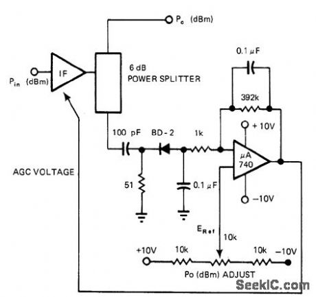
Low-pass filter serves as loop giving dosed-loop bandwidth of at least 5 kHz. Loop operates in square-law region of de-tector diode. Inputs to IF amplifier are in range from -60 dBm to -to dBm, and AGC action provides 30-MHz IF output of -15 dBm. Power splitter ensures that detector also operates at -15 dBm. Article gives design equations and performance curves.-R. S. Hughes, Design Au-tomatic Gain Control Loops the Easy Way. EDN Magazine, Oct, 5, 1978, p 123.128. (View)
View full Circuit Diagram | Comments | Reading(499)
| Pages:1213/2234 At 2012011202120312041205120612071208120912101211121212131214121512161217121812191220Under 20 |
Circuit Categories
power supply circuit
Amplifier Circuit
Basic Circuit
LED and Light Circuit
Sensor Circuit
Signal Processing
Electrical Equipment Circuit
Control Circuit
Remote Control Circuit
A/D-D/A Converter Circuit
Audio Circuit
Measuring and Test Circuit
Communication Circuit
Computer-Related Circuit
555 Circuit
Automotive Circuit
Repairing Circuit