
Circuit Diagram
Index 1219
40_kHz_ULTRASONIC_TRANSMITTER
Published:2009/6/30 3:23:00 Author:May
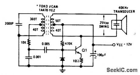
View full Circuit Diagram | Comments | Reading(970)
LOW_DRIFT_SAMPLE_AND_HOLD
Published:2009/6/30 3:22:00 Author:May
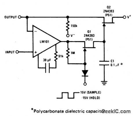
TheJFETs, Q1 and Q2, provide complete buffering to C1, the sample and hold capacitor.During sample, Q1 is turned on and provides a path, rds(on), for charging C1. During hold, Q1 is turned off, thus leaving Q1 ID(off) (<100 pA) and Q2 IGSS (< 100 pA) as the only discharge paths. Q2 serves a buffering function so feedback to the LM101 and output current are supplied from its source. (View)
View full Circuit Diagram | Comments | Reading(2147)
ULTRASONIC_PEST_REPELLER
Published:2009/6/30 3:22:00 Author:May
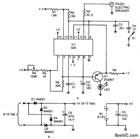
The device emits ultrasonic sound waves that sweep between 65,000 and 25,000 hertz. Designed around a 556 dual timer, one half operated as an astable nultivibrator with an adjustable frequency of 1 to 3 Hz. The second half is also operated as an astable multivibrator but with a fixed free running frequency around 45,000 Hz. The 25-65 kHz sweep is ac-complished by coupling the voltage across C2 (the timing capacitor for the first half of the 556) via Q1 to the control voltage terminal (pin 11) of the second half of the 556. The device that radiates the ultrasonic sound is a piezo tweeter. (View)
View full Circuit Diagram | Comments | Reading(5940)
25_W_logic_indicator_lamp_driver
Published:2009/7/24 11:44:00 Author:Jessie
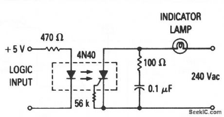
This circuit makes it possible to directly couple (without buffers) TTL and DTL inputs with either indicator or alarm devices. The optoelectronic coupling prevents both logic glitches and the introduction of noise. Motorola Thyristor Device Data, 1989, p. 6-20. (View)
View full Circuit Diagram | Comments | Reading(611)
BELL_SYSTEM_
Published:2009/6/30 3:22:00 Author:May
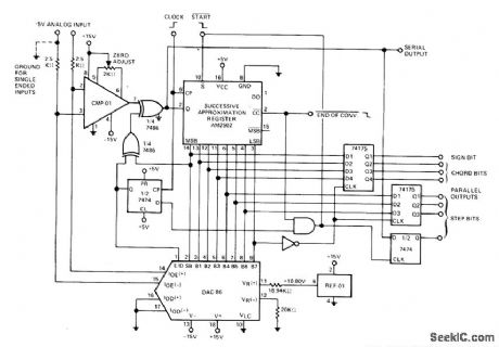
μ-255 COMPANDING LAW—Precision MonolithiCS DAa-86 is used in circuitthat provides 15-segment linear approximation by using 3 bits to select one of eight binarily related chords, then using 4 bits to select one of sixteen Iinearly related steps within each chord.Sign bit determines signal polarity, and encode/decode select bit determines operation, Circuit shown is for palallel data applications Forserialdata,omit inverter, two 74175 chips,and half of 7474 Power supplies should be well by-passed,— COMDAC Companding D/A Converter, Precision Monolithics, Santa Clara, GA, 1977, DAC-86,p 6. (View)
View full Circuit Diagram | Comments | Reading(665)
TTL_compatible_solid_state_relay
Published:2009/7/24 11:43:00 Author:Jessie
This circuit is compatible with 74, 74S, and 74H series TTL-logic inputs, and can handle 240 Vac loads up to 10 A. Motorola Thyristor Device Data, 1989, p. 6-20. (View)
View full Circuit Diagram | Comments | Reading(992)
M68000_microcomputer_interface
Published:2009/7/24 11:41:00 Author:Jessie
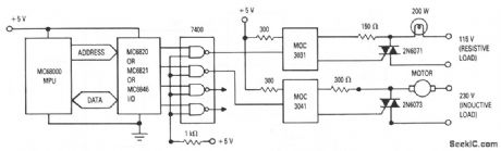
This circuit shows interface between an M68000 and resistive or inductive loads, using MOC3031 and MOC3041 optoisolators. The zero-crossing feature of these optoisolators extends life of incandescent lamps, reduces triac surge-current strains, and reduces EMI, as described for the circuit of Fig. 6-39 (but without the need for a timing circuit at the 7400 gate inputs). Motorola Thyristor Device Data, 1991, p. 1-6-16. (View)
View full Circuit Diagram | Comments | Reading(1806)
FOUR_OUADRANT_ALGEBRAIC
Published:2009/6/30 3:21:00 Author:May

Two Precision Monolithics DAC-08 D/A converters perform fast algebraic summation of two digital input words and feed OP-02 opamp that provides direct analog output which is algebraic sum of words A and B in all four quadrants.—J. Schoeff and D. Soderquist, Differential and Multiplying Digital to Analog Converter Applications, Precision Monolithics, Santa Clara, CA, 1976, AN-19, p 7. (View)
View full Circuit Diagram | Comments | Reading(1463)
M6800_microcomputer_interface
Published:2009/7/24 11:37:00 Author:Jessie
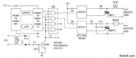
This circuit shows interface between an M6800 or M6802 and resistive or inductive loads. If the second input of the gates is tied to the optional timing circuit shown, the triacs will fire only at the zero crossing of the ac line voltage. This extends life of incandescent lamps, reduces surge-current strains on the triac, and reduces EMI generated by load switching-all without special software or programming within the processor. Motorola Thyristor Device Data, 1991, p. 1-6-14. (View)
View full Circuit Diagram | Comments | Reading(350)
MOS_to_ac_load_interface
Published:2009/7/24 11:33:00 Author:Jessie
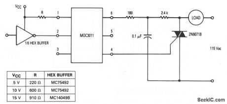
This circuit shows interface between MOS logic and an ac load, using an MOC3011 optoisolator with triac-driver output (chapter 9). The value of R depends on the type of MOS buffer used. Motorola Thyristor Device Data, 1991, p. 1-3-16. (View)
View full Circuit Diagram | Comments | Reading(1670)
Logic_to_inductive_load_interface
Published:2009/7/24 11:31:00 Author:Jessie
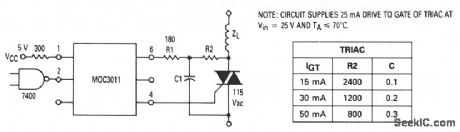
This circuit shows interface between conventional 7400 TTL logic and a triac, using an MOC3011 optoisolator with triac-driver output (chapter 9). The values of C and R2 depend on the triac current. Maxim, 1992, Appications and Product Highlights, p. 1-3-15. (View)
View full Circuit Diagram | Comments | Reading(685)
Fully_isolated_data_MUX
Published:2009/7/24 11:30:00 Author:Jessie
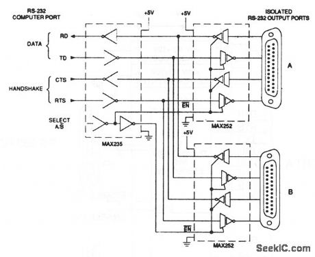
This fully-isolated RS-232 MUX allows a single RS-232 computer port, powered from 5 V, to drive one of two separate remotely located peripherals (typically a data-acquisition satellite and a remote printer). Isolation is useful here because both devices are likely to have ground potentials different from that of the computer. Also, the connection isolates the peripherals from each other as well as the computer. The MAX235 takes RS-232 data and handshake lines and a Select A/B output from the computer and converts them to logic levels. These levels are passed along to both MAX252 isolated transceivers. The RTS line controls which port is selected. Maxim, 1992,Appications and Product Highlights, p. 2-8. (View)
View full Circuit Diagram | Comments | Reading(1501)
Two_RS_232_serial_ports_with_one_chip
Published:2009/7/24 11:27:00 Author:Jessie
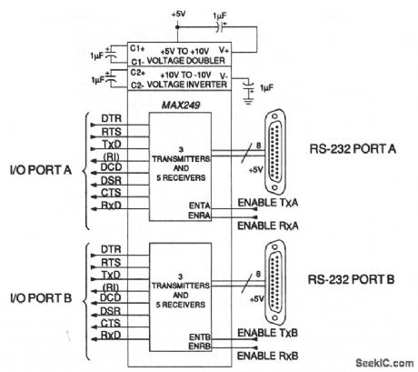
In this circuit, a MAX249 includes a full complement of drivers and receivers for two complete DTE (Data Terminal Equipment) serial ports. The circuit also saves power with separate shutdown inputs for the inputs and outputs of both DTE ports. When both ports are off, supply current is only 25μA. The dual serial ports are powered from a single +5-V supply. The guaranteed data rate is 64 kb/s, which ensures compatibility with EIA-232D/232E, V.28/V.24, and EIA-562. Maxim, 1992, Appications and Product Highlights, p. 2-6. (View)
View full Circuit Diagram | Comments | Reading(542)
PEAK_DETECT_AND_HOLD
Published:2009/6/30 3:20:00 Author:May
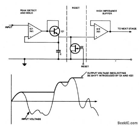
If the voltage at the input exceeds the voltage on the capacitor, then the output of the 741 goes positive, the diode conducts, and the capacitor is charged up to the input voltage-forward voltage drop of diode. When the voltage at the input is less than that on the capacitor, the output of the 741 goes negative, and the diode cuts off. To prevent the capacitor from discharging through the input resistance of the next stage, a high input impedance buffer stage (IC2) is used. The circuit can be reset by means of a FET or similar high impedance device connected across the capacitor. (View)
View full Circuit Diagram | Comments | Reading(945)
Four_14_bit_outputs_from_one_DAC
Published:2009/7/24 11:23:00 Author:Jessie
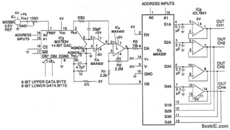
In this circuit, the low-leakage performance of a MAX329 provides an economical way to create four 14-bit DAC outputs from only one 14-bit DAC. Four 0.1-μF capacitors and an ICL7641 quad op amp sample the DAC voltage that is presented by the MUX. The A-section of the MAX329 scans the hold capacitors, while the B section closes a feedback loop, which connects the appropriate buffer within IC6 to a precision op amp (IC4). This loop effectively removes the buffer offset voltage. If a typical MUX charge injection of the 4 pC and a typical leakage (plus op-amp bias) of 1 pA are assumed, the voltage stored on each capacitor drops no more than 1 bit (out of 214) over 2.5 seconds at 25℃ . Maxim, 1992, Appications and Product Highlights, p. 9-5. (View)
View full Circuit Diagram | Comments | Reading(561)
ELECTRONIC_COMBINATION_LOCK
Published:2009/6/30 3:17:00 Author:May

Switches S1 through S5 must be operated In rapid sequence to operate the lock,They can be any numbers on a 10-button switch pad.If an Incorrect button is pushed,alarm sounds and the circuit is disabled for two minutes. (View)
View full Circuit Diagram | Comments | Reading(1)
POWER_FAILURE_ALARM_1
Published:2009/6/30 3:16:00 Author:May

While the power is on,the relay is held open,but when the power fails the buzzercircuit contacts close. (View)
View full Circuit Diagram | Comments | Reading(622)
AUTOREFERENCE
Published:2009/6/30 3:15:00 Author:May
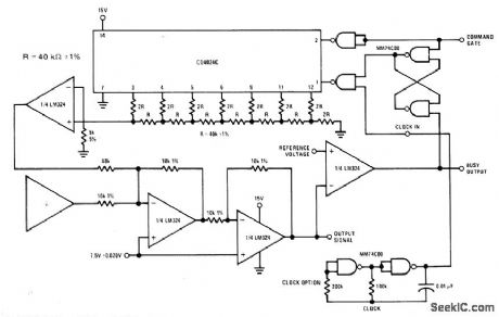
National CD4024C coni verter is used with logic and summer elements to elim inate virtually all offset errors induced by time and temperature changes in process coni trol system fed by transducer. Best suited for applications having short repeated duty cycles, each containing reference point. Examples indude weighinga scalein which transducer is load cell, pressure control systems, fuel pumps, and sphygmomanometers. Circuit eliminates warm-up emors.— Pressure Transducer Hand-book, National Semiconductor, Santa Clara, CA, 1977, p 7-4-7-8. (View)
View full Circuit Diagram | Comments | Reading(552)
POWER_FAILURE_DETECTOR
Published:2009/6/30 3:15:00 Author:May

This circuit indicates that a power outage occured for with the values given for R* and C*. After a power failure, pushing the Reset button. (View)
View full Circuit Diagram | Comments | Reading(1012)
Voltage_output_DAC
Published:2009/7/24 11:19:00 Author:Jessie
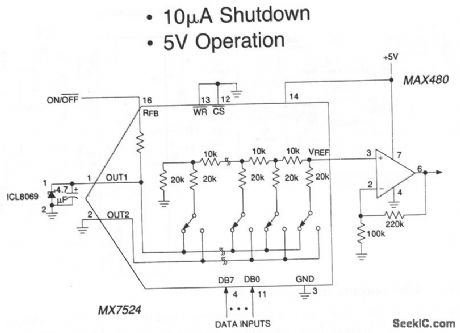
In this circuit, an MX7524 8-bit current output DAC is connected in an inverted configuration (voltage mode) by driving the IOUT pin with a 1.23-V reference (ICL8069). The DAC output drives a MAX480 where the gain is set so that full-scale output is 4 V. The power consumption is below 1 mW (operating) and much less shut down. The circuit operates when the On/Off input is at 5 V. When On/Off is at 0 V, supply current falls to 15μA, and the amplifier output falls to 0 V. The DAC input data can be retained if the WR input is used. Digital input lines must be driven with CMOS logic levels (rail-to-rail) to minimize supply current. Maxim, 1992,Appications and Product Highlights, p. 8-15. (View)
View full Circuit Diagram | Comments | Reading(833)
| Pages:1219/2234 At 2012011202120312041205120612071208120912101211121212131214121512161217121812191220Under 20 |
Circuit Categories
power supply circuit
Amplifier Circuit
Basic Circuit
LED and Light Circuit
Sensor Circuit
Signal Processing
Electrical Equipment Circuit
Control Circuit
Remote Control Circuit
A/D-D/A Converter Circuit
Audio Circuit
Measuring and Test Circuit
Communication Circuit
Computer-Related Circuit
555 Circuit
Automotive Circuit
Repairing Circuit