
Circuit Diagram
Index 1221
ANALOG_SUM_OF_DIGITAL_NUMBERS
Published:2009/6/30 3:04:00 Author:May

Two Precision Monolithics DAC-100 D/A convelters and op-01 opamp combine conversion with adding to give high-precision DC output voltage,200-ohm pots are adjusted initially to give exactly desired output for input of all 0s,— 8 &10 Bit Digital-to-Analog Converter, Precision Monolithics, Santa Clara, CA, 1977、DAC-100, p 5. (View)
View full Circuit Diagram | Comments | Reading(848)
COLPITTS_OSCILLATOR
Published:2009/6/30 3:04:00 Author:May

When calculating its resonan frequency,use C1C2/C1+C2 for the total capacitance ofthe L-C circuit. (View)
View full Circuit Diagram | Comments | Reading(0)
LOW_VOLTAGE_FLASHER
Published:2009/6/30 3:02:00 Author:May

Circuit Notes
Applying voltage to the circuit triggers SCR1. With SCR1 on, the voltage on the anode of SCR2 rises until SCR2 triggers to commu-tate SCR1. The voltage on the gate of SCR1 will swing negative at this time, and only after a positive potential of 0.5 volt is once again attained, will SCR1 retrigger. The circuit could be used for higher voltage levels, but the peak negative voltage on the gate of SCR1 must be limited to less than 6 volts. (View)
View full Circuit Diagram | Comments | Reading(879)
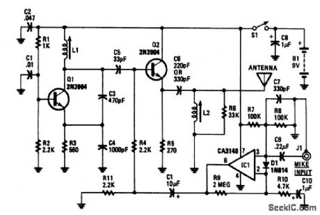
1_2_MHz_BROADCAST_TRANSMITTER
Published:2009/6/30 3:02:00 Author:May
T1 is a low impedance output transformer 5000-8 ohms. (View)
View full Circuit Diagram | Comments | Reading(963)
2_DIGIT_BCD_INPUT
Published:2009/6/30 3:01:00 Author:May

Each Signetics 5007/5008 multiplying D/A convener serves one digh of input voltage to give output current that is product of digital input number and input reference current,Opamp combines currents and converts them to analog output voltage proportional to digital input value.—Signetics Analog Data Manual, Signetics, Sunnyvale, CA, 1977, p 677-685. (View)
View full Circuit Diagram | Comments | Reading(582)
27_MHz_AND_49_MHz_RE_OSCILLATOR_TRANSMITTER
Published:2009/6/30 3:00:00 Author:May

The modulator and oscillator consist of two NPN transistors. The base of the modulator transistor is driven by a bidirectional current source with the voltage range for the high condition limited by a saturating PNP collector to the pin 4 VREG voltage and low condition limited by a saturating NPN collector in series with a diode to ground. The crystal oscillator/transmi tter transistor is configured to oscillate in a class C mode. Because third overtone crystals are used for 27 MHz or 49 MHz applications a tuned collector load must be used to guarantee operation at the correct frequency. (View)
View full Circuit Diagram | Comments | Reading(1502)
DAC_FOR_SPEECH
Published:2009/6/30 3:00:00 Author:May

Audio signals stored in 8-channel digital form in computer are converted back into analog form for feed through low-pass filter to input of audio amplifier. Can be used for computer-controlled synthesis of speech from phonemes in any language or for providing voice replies to queries. Pin 7 of IC9 is +12 V, and pin 4 is -12V.—S. Ciarcia, Talk to Me! Add a Voice to Your Computer for $35, BYTE, June 1978, p 142-151 (View)
View full Circuit Diagram | Comments | Reading(1489)
DC_FLASHER_WITH_ADJUSTABLE_ON_AND_OFF_TIME
Published:2009/6/30 2:59:00 Author:May

Circuit NotesThis circuit utilizes a power flip-fl。p and programmable unijunction(PUT)to obtainadjustable on and off times. (View)
View full Circuit Diagram | Comments | Reading(972)
6_BITS_TO_ANALOG
Published:2009/6/30 2:59:00 Author:May

Uses Motorola MC1723G voltage regulator to provide reference voltage and opamp for MC1406L 6-bit D/A converter. Output cument can be up to 150 mA. Full-scale output is about 10 V, but can be boosted as high as 32V by increasing value of R2 and increasing +15 V supply proportionately to maximum of 35 V.—D. Aldridge and K. Huehne, 6-Bit D/A Converter Uses Inexpensive Components, EDN Magazine, Dec. 15, 1972, p 40-41. (View)
View full Circuit Diagram | Comments | Reading(667)
Precision_voltage_regulrttor_controller
Published:2009/7/24 20:10:00 Author:Jessie

In this circuit, the ICL8212 is used as the controller for a highly-stable series voltage regulator. The output voltage is simply programmed, using resistor divider network R1/R2. C1 and C2 are required to ensure stability because the ICL8212 is not compensated internally. This regulator system can be used with lower input voltages and it consumes less power for a given output control current than most commercial regulators. Thus, the circuit is most useful for battery-powered systems that operate at low voltages. (View)
View full Circuit Diagram | Comments | Reading(656)
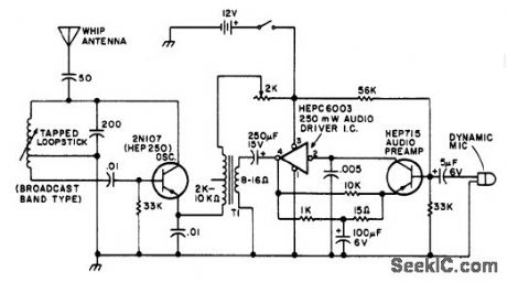
WIRELESS_AM_MICROPHONE
Published:2009/6/30 2:59:00 Author:May
Transistor Q1 and its associated components comprise a tuneable rf oscillator. The rf signal is fed to transistor Q2, the modulator. Operational amplifier IC1 increases the audio signal and applids it through resistor R4 to the base of Q2. Tune an AM radio to an unused frequency between 800 to 1600 kHz. Tune L1 for a change in the audio level coming from the radio. Peak the output by adjusting L2. If L1 is disturbed, it may be necessary to readjust L2 for peak performance. Depending on the impedance of the microphone audio sensitivity can be increased by decreasing the value of R10 and vice versa. (View)
View full Circuit Diagram | Comments | Reading(1076)
Constant_current_source
Published:2009/7/24 20:08:00 Author:Jessie

The ICL8212 and ICL8211 provide constant current sources of 25 and 130 μA, respectively, when connected as shown. The equivalent parallel resistance is in the tens of megohms over the supply-voltage range from 2 to 30 V. (View)
View full Circuit Diagram | Comments | Reading(1)
Programmable_Zener_voltage_reference
Published:2009/7/24 20:07:00 Author:Jessie


In this circuit, an ICL8212 stimulates a Zener diode by connecting the output terminal (pin 4) to the VZ output, and using a resistor network connected at the VTH terminal (pin 3) to program the Zener voltage. Power (V+) is applied to pin 8, with pin 5 connected to ground. The zener voltage is calculated by:
Because there is no internal compensation, the 5-μF capacitor is required across the output to prevent oscillation. Zener voltages from 2 to 30 V can be programmed. Typical impedance values between 300 μA and 25 mA range from 4 to 7Ω. The Zener knee is sharper and occurs at a significantly lower current than similar devices. (View)
View full Circuit Diagram | Comments | Reading(688)
9_BIT_USING_DIGITAL_SWlTCHES
Published:2009/6/30 2:58:00 Author:May

Combination of CD4007A multiple-switch CMOS ICs, ladder network of discrete metal-oxide film resistors, CA3160 voltage-follower opamp, and CA3085 voltage regulator gives digital-to-analog converter that is readily interfaced with 10-V logic levels of CMOS input. Required resistor accuracy, ranging from ±0.1% for bit 2 to ±1% for bits 6-9, is achieved by using series and parallel combinations of 806K resistors.— Linear Integrated Circuits and MOS/FET's, RCA Solid State Division, Somerville, NJ, 1977, p 267-268. (View)
View full Circuit Diagram | Comments | Reading(857)
Low_offset_12th_order_max_flat_low_pass_filter
Published:2009/7/24 13:09:00 Author:Jessie

This circuit shows a 12th-order filter that uses two LTC1062s and a precision dual op amp. Figure 7-16B shows the frequency response for the following values: fc=4 kHz, R=59 kΩ, C=0.001μF, R'=5.7 kΩ, C'=0.01 μF, R1=R2=39.8 kΩ, C1=2000 pF, C2=500 pF, fclock=438 kHz. Linear Technology Corporation, Linear Applications Handbook, 1990, p. AN20-8, -9. (View)
View full Circuit Diagram | Comments | Reading(547)
Cascaded_IC_low_pass_filters
Published:2009/7/24 13:07:00 Author:Jessie

Figure 7-15A shows two LTC1062 filters where the second input is taken directly from the dc-accurate output of the first filter. The recommended ratio of R'/R is about 117/1, 1/(6.28RC) should equal fc/1.57, and 1/(6.28R'C') should equal fc/1.6 when the filters are cascaded (Fig. 7-15A). For example, for an fc of 4.16 kHz, the clock should be 416 kHz, and R=909 Ω, R'=107 kΩ, C=0.066 pF, and C'=574 pF. Figure 7-15B shows cascaded filters where the second input is taken from the buffered output of the first filter. The recommended values for R and C are determined by: 1/(6.28RC) =fc/1.59 and 1/(6.28R'C')=fc/1.64 when the filters are cascaded as shown in Fig. 7-15B. For example, for an fc of 4kHz, the values should be: R=97.6 kΩ, C=616 pF, R'=124 kΩ, and C'=508 pF. Linear Technology Corporation, Linear Applications Handbook, 1990, p. AN20-7. (View)
View full Circuit Diagram | Comments | Reading(540)
NEON_TUBE_FLASHER
Published:2009/6/30 2:57:00 Author:May

The voltage required to ignite the neon tube is obtained by using an ordinary filament transformer (240-6.3 V) in reverse. Battery drain is quite low, around 1 to 2 milliamps for a nine volt battery. The pulses from Q1, uni-junction transistor, operated as a relaxation oscillator and are applied to Q2 which in turn drives Q3 into saturation. The sharp rise in current through the 6.3 V winding of the trans-former as Q3 goes into saturation induces a high voltage in the secondary winding causing the neon to flash. The diode Dl protects the transistor from high voltage spikes generated when switching currents in the transformer. (View)
View full Circuit Diagram | Comments | Reading(885)
IC_Iow_pass_filter
Published:2009/7/24 13:05:00 Author:Jessie
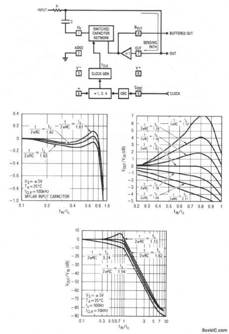
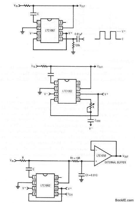
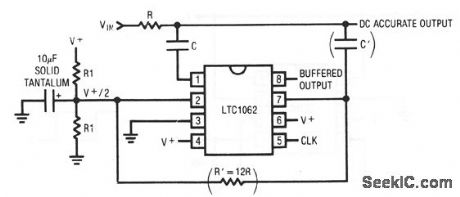
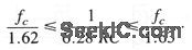


Figure 7-14A shows the architecture and basic connections for an LTC1062 low-pass filter (similar to a 5th-order Butterworth). The cutoff frequency fc (at the -3-dB point) is determined by the values of R and C, with the relationship:
The clock frequency should be 100 times fc,. Figure 7-14B shows the passband response for values of 1/(6.28RC) near fc/1.62. Figures 7-14C and 7-14D are similar, but with a wider range of values. Figure 7-14D shows the LTC1062 operated from a single supply and an external CMOS clock signal. Figure 7-14F shows the LTC1062 operated with the internal clock. If COSC is 8500 pF and a 50-kΩ pot is connected to pin 5, the clock frequency can be adjusted from 500 Hz to 3.3 kHz (providing for an fc of 5 to 33 Hz). Figure 1-14G shows how an extemal buffer can be connected to the LTC1062 to eliminate clock feedthrough and improve the high-frequency attenuation floor. Figure 7-14H shows how the LTC1062 can be operated from a single supply , Linear Technology Corporation, Linear Applications Handbook, 1990, p. AN20-1, -2, -3, -4.
(View)
View full Circuit Diagram | Comments | Reading(722)
Single_2nd_order_filter_section
Published:2009/7/24 12:59:00 Author:Jessie

The MAX274/275 continuous-filter architecture uses a four-amplifier state-variable design. The on-chip capacitors and amplifiers, together with external resistors, form cascaded integrators with feedback to provide simultaneous low-pass and bandpass filtered outputs. The low-pass and bandpass frequencies, as well as filter Q, are determined by external resistor values, using the equations shown. No external capacitors are needed. On-chip capacitors are factory trimmed to provide better than 1% pole-frequency accuracy over the temperature range. ±1%-tolerance resistors provide ±2%-accurate pole frequencies. Accurate filter Qs can also be obtained by compensating for amplifier bandwidth limitation using the graphs that are provided on the data sheet. Maxim, 1992, Applications and Product Highlights, p. 7-3. (View)
View full Circuit Diagram | Comments | Reading(1191)
Power_on_reset_generator
Published:2009/7/24 12:41:00 Author:Jessie
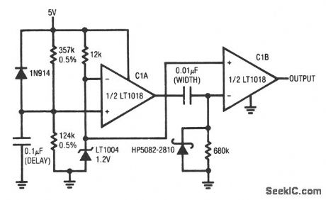
This circuit uses both sections of an LT1018 to reset a digital system after supply turn-on. When supply power is applied, the 5-V rail comes up. The LT1004 clamps at 1.2 V and the C1A noninverting input ramps at a time constant that is determined by the 0.05% resistors and the 0.1-μF capacitor. When the C1A noninverting input ramps beyond the LT1004 potential, the C1A output goes high and delivers a differentiated pulse to the C1B inverting input. The C1B output goes low for a period that is determined by the 0.01-μF/680-kΩ differentiator. The 1N914 gives quick reset for the 0.1-μF capacitor, and the Schottky diode clips differentiator-caused negative voltages at the C1B input. The turn-on threshold (4.8 V in this case) is set by the ratio of the 0.5% resistors. The output-pulse delay time is controlled by the 0.1-μF capacitor, which can be varied. Similarly, the RC combination at C1B sets output pulse width, and can be varied. The LT1018 1.2-V minimum supply voltage prevents spurious output during supply power-up. Linear Technology, Linear Applications Handbook, 1990, p. AN31-10. (View)
View full Circuit Diagram | Comments | Reading(760)
| Pages:1221/2234 At 2012211222122312241225122612271228122912301231123212331234123512361237123812391240Under 20 |
Circuit Categories
power supply circuit
Amplifier Circuit
Basic Circuit
LED and Light Circuit
Sensor Circuit
Signal Processing
Electrical Equipment Circuit
Control Circuit
Remote Control Circuit
A/D-D/A Converter Circuit
Audio Circuit
Measuring and Test Circuit
Communication Circuit
Computer-Related Circuit
555 Circuit
Automotive Circuit
Repairing Circuit