
Circuit Diagram
Index 1230
Basic_Wien_bridge_sine_wave_oscillator
Published:2009/7/24 20:27:00 Author:Jessie
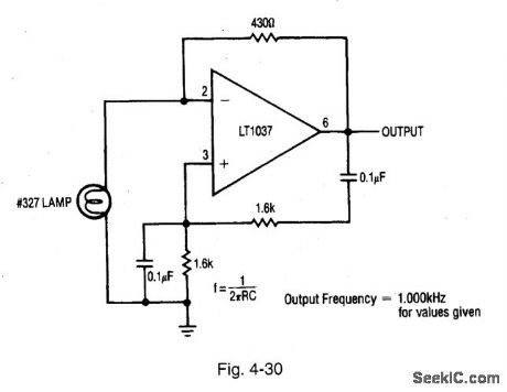
Figure 4-30 shows a Wien-bridge sine-wave oscillator with a lamp in one leg of the bridge(similar to that of Figs,4-26 and 4-28).LINEAR TECHNOLOGY,APPLICATION NOTE 43,P. 29. (View)
View full Circuit Diagram | Comments | Reading(689)
FAIL_SAFE_TIMED_ALARM
Published:2009/6/30 1:53:00 Author:May

Horn comes on about 30 s after intruder closes door switch by opening car door. Delay is produced by NE555 timer to allow driver to close door after entering or leaving. Thief must keep door open to get leg room for removing equipment under dash. Diodes are 50-PIV 1-A silicon. K1 has 12-V coil. Alarm is set at all times. S1 is normally dosed pushbutton type in door jam. Opening S1 starts timer, and closing it resets alarm.-R. S. Harvey, Junk Box Foils Thieves, QST, Sept. (View)
View full Circuit Diagram | Comments | Reading(920)
FOUR_CHANNEL_MIXER
Published:2009/6/30 1:53:00 Author:May
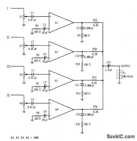
All four sections of RCA CA3048 quad differential amplifier are utilized in linear mixer providing gain of 20 dB for each channel. Designed for use with load of 10K or larger. All inputs are high impedance.-E. M Noll, Linear IC Principles, Experiments, and Projects, Howard VV. Sams, Indianapolis, IN, 1974, p 173 and 179. (View)
View full Circuit Diagram | Comments | Reading(0)
8_BIT_TRACKING
Published:2009/6/30 1:52:00 Author:May
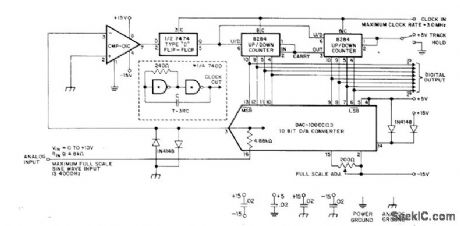
Uses Precision MonolithIcs DAC-100 CCQ3 D/A converter and CMP-01CJ fast precision comparator to make digital data contiguously available at output while tracking analog input. Diode clamps hold DAC output near zero despite input and turn-on transients.Unused least significant digital inputs of 10-bit DAC are turned off by connecting to +5 V as shown. Simple clock circuit shown in dashed box is stable over wide range of temperatures and supply voltages. D/A ionverter is used in feedback configuration to obtain A/D opera-tion.— A Low Cost, High-Performance Tracking A/D Converter, Precision Monolithics, Santa Clara, CA, 1977, AN-6.P 2. (View)
View full Circuit Diagram | Comments | Reading(748)
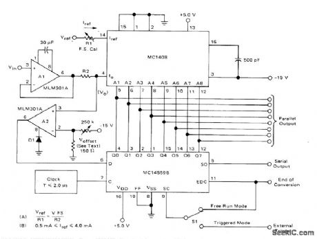
CMOS_COMPATIBLE_SUCCESSIVE_APPROXI_MATION
Published:2009/6/30 1:51:00 Author:May
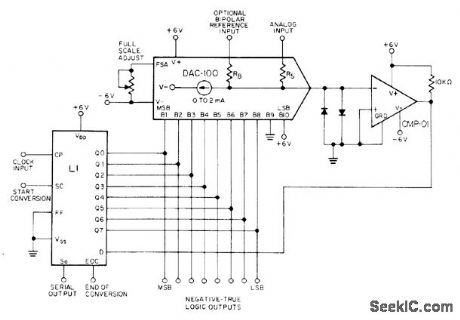
Converts analog inputto 8-bit digital output by using MC14559 CMOS successive-approximation registerwith Precision Monolithics DAC-100 D/A converter and CMP-01 comparator. Conversion sequence is initiated by applying positive pulse, with width greaterthan one clock cycle, to START CONVERSION input. Analog input is then compared successively to 1/2 scale, 1/4 scale, and remaining binarily decreasing bit weights until it has been resolved within 1/2 LSB. END OF CONVERSION then changes to logic 1 and parallel answer is present in negative-true binary-coded format at register outputs.—D. Soderquist, Interfacing Precision Monolithics Digital-to-Analog Converters with CMOS Logic, Precision Monolithics, Santa Clara, CA, 1975, AN-14, p 4. (View)
View full Circuit Diagram | Comments | Reading(1025)
COMPRESSING_A_D_CONVERSION
Published:2009/6/30 1:50:00 Author:May

Step size increases as output changes from zero scale to full scale, in contrast to conventional linear converter in which step size is constant percentage of full scale. Uses Precision MonolithIcs DAC-76 D/A converter in combination with CMP-01 comparator, any standard EXCLUSIVE-OR gate, and successive-approximation register for conversion logic. Encoding sequence begins with sign-bit comparison and decision. Bits are con verted with successive-removal technique, starting with decision at code 011 1111 and turning off bits sequentially until all decisions have been made. Conversion is completed in nine clock cycles.— COMDAC Companding D/A Converter, Precision MonolithIcs, Santa Clara, CA, 1977, DAC-76, p 12. (View)
View full Circuit Diagram | Comments | Reading(1121)
The night lock automatic lamp circuit
Published:2011/7/5 1:19:00 Author:zj | Keyword: The night lock, automatic lamp circuit

When you come back from the outside, it is so dark that unlocking is not unconvenient. As shown in the diagram it is a automatic lamp. When the key touches the door, the small lamp will light up automatically. After getting in the room indoor lamp will light up at the same time. At this time you can easily turn it on, the door lamp will automatically extinguish 20s later. Automatic lamp circuit is as shown in the figure. (View)
View full Circuit Diagram | Comments | Reading(654)
Quartz_stabilized_bridge_oscillator_with_common_mode_suppression
Published:2009/7/24 20:25:00 Author:Jessie

Figure 4-28 shows a bridge-oscillator circuit where the common-mode swing is suppressed by the addition of a second amplifier. This configuration forces the bridge midpoint to virtual ground by measuring the midpoint value and comparing it to ground. Because the bridge drive is complementary, the oscillator amplifier sees no common-mode swing, thus reducing distortion. Figure 4-29 shows less than 0.005% distortion(trace B)in the output(trace A)waveform.(Distortion measurements are covered In Chapter 6.) Lnvean TECHNOLOGY,APPLICATION Nom 43,P. 28. (View)
View full Circuit Diagram | Comments | Reading(564)
TONE_CONTROL_WITH_HIGH_INPUT_IMPED_ANCE
Published:2009/6/30 1:48:00 Author:May

Use of 2N5458 JFET ahead of opampfeedback-type tone control provides high input impedance and low noise characteristics for high-fidelity audio applications,- FET Databook,″ National Semiconductor, Santa Clara、CA、1977,p 6-26-6-36 (View)
View full Circuit Diagram | Comments | Reading(786)
Improved_5_V_power_supply_monitor
Published:2009/7/24 20:22:00 Author:Jessie

This circuit is an improved version of the circuit shown in Fig. 9-33. The calibration procedure is the same. (View)
View full Circuit Diagram | Comments | Reading(723)
8_BIT_SUCCESSIVE_APPROXIMATION
Published:2009/6/30 1:48:00 Author:May
Requires only four ICs. For each cycle, most significant bit is enabled first, with comparator giving output signifying that input signal is greater or less in amplitude than output of Motorola MC1408. If output is greater, bit is reset or turned off. Process is repeated for next most significant bit until all bits have been tried, completing conversion cyde. Conversion time is 18 μs, total propagation delay is about 1.5 μs, and ovorall operational figure is about 2 μS per bit for 8-bit system.—T.Henry, Successive Approximation A/D Coversion, Motorola、Phoenix、AZ,1974、AN-716、p 4. (View)
View full Circuit Diagram | Comments | Reading(628)
5_V_power_supply_monitor
Published:2009/7/24 20:20:00 Author:Jessie

This circuit uses an LM3914 bar/dot display driver and 10 LEDs to form a simple power-supply monitor.To calibrate,set VCC at 5.41V and adjust R6 until LED9 and LED 10 are equally illuminated.Disconnect R1 from VCC,but leave D1 connected to VCC.Connect R1 to 4.500V,and adjust R4 until LED 1 just barely turns on.Readjust R6 and R1 as necessary. (View)
View full Circuit Diagram | Comments | Reading(680)
AUTOMATlC_LEVEL_CONTROL
Published:2009/6/30 1:48:00 Author:May

Uses Signetics NE570 or NE571 analog compandor to provide automatic level control for audio signal processing, to give constant high percentage modulation despite varying input levels. Optional resistor Rx varies threshold of level regulation. Widest range of gain control is obtained with Rx, open. When resistor value is Iowered, larger input signal is required for full output.Peak-level dipping with pair of reverse paralleled LEDs controls overshoots on speech by limiting RMS output to 2.2 V P-P. Ry regulates dipped amplitude.-W. G. Jung, Gain Control IC for Audio Signal Processing. Ham Radio, July 1977, p 47-53. (View)
View full Circuit Diagram | Comments | Reading(4573)
Precision_current_sensing_in_supply_rails
Published:2009/7/24 20:14:00 Author:Jessie

This circuit shows an LTC1043 (Fig. 1-4B) connected to sense current through a shunt in either of the supply rails. This capability has wide application in battery and solar-powered systems (chapter 8). If the ground-referred voltage output is unloaded by an amplifier, the shunt can operate with very little voltage drop across it, which minimizes losses. (View)
View full Circuit Diagram | Comments | Reading(595)
Voltage_controlled_current_source
Published:2009/7/24 20:14:00 Author:Jessie

This circuit shows an LTC1043 (Fig. 1-4B) connected as a voltage-controlled current source with ground-referred input and output. Bipolar sup-plies will permit bipolar output. Configurations featuring a grounded voltage-control source and a grounded load are usually more complex and they depend on several components for stability. In this circuit, accuracy and stability almost entirely depend on the 100-Ω shunt. (View)
View full Circuit Diagram | Comments | Reading(0)
2_DIGIT_BCD
Published:2009/6/30 1:48:00 Author:May
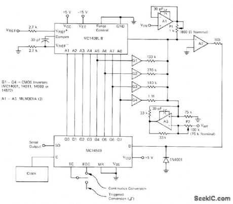
Uses Motorola MC14549 successive-approximation register and MC1408L-8 D/A converter to give full-scale value of 0.99 V in 10-mV increments. Input is buffered by opamp A1 connected as voltage follower, with pot P1 set to give output current proportional to un-known input voltage. This current is compared to that required by total BCD A/D converter. Pins 1-4 and 12-15 of MC14549 provide required 2-digit parallel BCD output. Clock frequency can be 100 kHz.-D. Aldridge, Successive Approximation BCD AiD Converter, Motorola, Phoenix, AZ, 1975, EB-51. (View)
View full Circuit Diagram | Comments | Reading(1424)
Step-down converting power circuit composed Of MC34063
Published:2011/5/5 20:03:00 Author:May | Keyword: Step-down, converting power

Step-down Vary Power Circuit Composed ofMC34063 is shown in the diagram. MC34063 is a type of switching modehighly active DC/DC Changed circuits. Its internalincludes reference voltage source withthe function of temperature compensation, comparator, duty ration controllable oscillator with limited current circuit, driver and heavy current output switch tube. The +25V/+5V step-down vary power composed of it is shown in the picture, the features are: (VIN=25V when IO=500mA) line regulation is 12mV±0.12%; load regulation is 3mV±0.03%; ripple voltage is 120mV. If one-level filter (shown in figure) output ripple reduced to 40mV; conversion efficiency is 82%; short-circuit limiting current is 1.1A.
(View)
View full Circuit Diagram | Comments | Reading(6224)
OCTAVE_EaUALIZER
Published:2009/6/30 1:47:00 Author:May

Provides ten bands of tone control, separated by one octave in frequency, with independent adjustment for each.Used to compensate for unwanted amplitudefrequency or phase-frequency characteristics of audio systems. Values of C1 and C2 for each circuit are given in table. With control R2 in flat position, circuit becomes all-pass with unity gain.Moving R2 to full boost gives bandpass characteristic, and moving in other direction to full cut gives bandreject or notch filter. For stereo, identical equalizer is needed for other channel.- Audio Handbook, National Semi-conductor, Santa Clara, CA, 1977, p 2-53-2-59 (View)
View full Circuit Diagram | Comments | Reading(699)
HIGH_SPEED_SUCCESSIVE_APPROXIMATION
Published:2009/6/30 1:46:00 Author:May

Total converslon time for 8-bit system is about 4.5 μs,clock rate is up to 2 MHz. Serial output is used for transmission to one or more other location. —T. Henry, Successive Approximation A/D Conversion, Motorola, Phoenix, AZ, 1974, AN-716, p 5. (View)
View full Circuit Diagram | Comments | Reading(1307)
BCD_OUTPUT
Published:2009/6/30 1:45:00 Author:May
Latched nonmultiplexed paral lel BCD outputs from Teledyne 8750 3 1/2-digit CMOS analog-to-dighal converter are suitable for liquid crystal and gas-discharge displays. 2-mA drain on 15 V supply permits battery operation. Features include high linearity, noise immunity, and 3 1/2-digit resolution within 0.025% error. Circuit is based on switching number of cument pulses needed to bring analog current to zero at input of opamp, then detarmining digital equivalent by counting these pulses. Values shown are for full-scale voltage input of 10 V and voltage reference of -6.4 V.—CMOS A-D Converter Provides BCD Output, Computer Design, Nov. 1977, p 156 and 158. (View)
View full Circuit Diagram | Comments | Reading(574)
| Pages:1230/2234 At 2012211222122312241225122612271228122912301231123212331234123512361237123812391240Under 20 |
Circuit Categories
power supply circuit
Amplifier Circuit
Basic Circuit
LED and Light Circuit
Sensor Circuit
Signal Processing
Electrical Equipment Circuit
Control Circuit
Remote Control Circuit
A/D-D/A Converter Circuit
Audio Circuit
Measuring and Test Circuit
Communication Circuit
Computer-Related Circuit
555 Circuit
Automotive Circuit
Repairing Circuit