
Circuit Diagram
Index 1220
MOSQUITO_REPELLING_CIRCUIT
Published:2009/6/30 3:14:00 Author:May
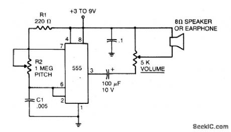
In the 555 oscillator circuit, adjusting R2 will provide output frequencies from below 200 Hz to above 62 kHz. Use a good quality miniature speaker so that it will produce frequencies on the order of 20 kHz. (View)
View full Circuit Diagram | Comments | Reading(752)
Square_root_circuit
Published:2009/7/24 11:09:00 Author:Jessie
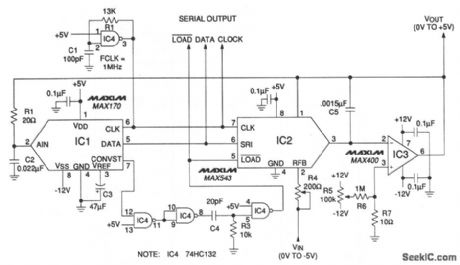
In this circuit, a 12-bit MAX543 DAC and a MAX170 A/D operate in the feedback loop of a single op amp to determine the square-root or a 0- to -5-V input signal. Both analog (VOUT) and digital outputs (serial DATA output) are provided. Accuracy surpasses 0.1% for -5-mV to 5-V inputs. The MAX543 squares the op-amp input, with an output that is proportional to IOUT=VREF(DAC code) +VIN. One DAC multiplying input is digital. The MAX170 A/D digitizes the op-amp output and transmits 12-bit data to the DAC. Consequently, the DAC VREF input and digital input carry the same value. The DAC output is then: IOUT=√5 ×√-VIN . Typical input/output examples are: VIN=-5.000 V, VOUT=+5.000 V; VIN=-0.5 mV, and VOUT=+50 mV. Maxim, 1992,Appications and Product Highlights, p. 8-14. (View)
View full Circuit Diagram | Comments | Reading(1352)
CURRENT_CONVERTER
Published:2009/6/30 3:14:00 Author:May

Converts 8-bit TTL digital inputs to process current in range of 4 to 20mA, for microprocessor control of industrial operations. Fixed 0.5-mA current is added to DAC output current varying between0 and 2.0 mA and multiplied by factor of 8 to produce final output current of 4-20 mA. To calibrate, connect ammeter between output and ground, then apply +23 V ± 7 V and -5 V ± 1 V to converter. Make digital inputs all 0s (less than +0.8 V). Adjust R1 until output current is 4.0 mA.Changedigital inputs to all is (greater than +2.0 V), and adjust R2 until output current is 20 mA.—D. Soderquist, Build Your Own 4-20 mA Digital to Analog Converter, Instruments & Control Systems, March 1977, p 57-58. (View)
View full Circuit Diagram | Comments | Reading(1024)
Fault_protected_8_channel_18_bit_dynamic_range_A_D_converter
Published:2009/7/24 10:54:00 Author:Jessie
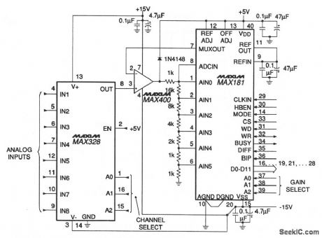
In this circuit, the MAX181 internal MUX forms a programmable-gain amplifier (PGA) with digitally-selected gains of 1, 2, 4, 8, 16, 32, 64, and 128. An external fault-protected MUX, the MAX378, selects from 8 input channels and protects the input for up to ±60-V voltage levels. Maxim, 1992, Appications and Product Highlights, p. 8-9. (View)
View full Circuit Diagram | Comments | Reading(542)
ULTRASONIC_BUG_CHASER
Published:2009/6/30 3:14:00 Author:May
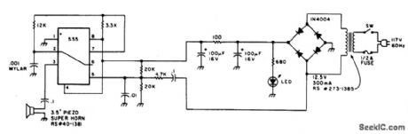
Low-intensity ultrasonic sound waves in the 30-45 kHz frequency band repel insects and small rodents. The unit is designed to generate a swept square wave from 30 to 45 kHz. The LM555 IC is wired as an ultrasonic oscillator driving a piezoelectric speaker of the hi-fi super-tweeter type. The output of the oscil-lator is swept by a 60-Hz signal from the ac input of the bridge rectifier. The LED acts as a pilot. (View)
View full Circuit Diagram | Comments | Reading(910)
AC_HOT_WIRE_PROBE
Published:2009/6/30 3:13:00 Author:May
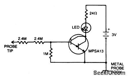
Insert the probe tip into either terminal of an ac outlet and hold the probe body against 3V anything that the circuit ground is connected to. The LED wi11 glow when the hot terminal is touched. Two 2.4 M resistors are used in the probe tip for safety (redundancy) reasons. (View)
View full Circuit Diagram | Comments | Reading(608)
ULTRASONIC_SWITCH
Published:2009/6/30 3:12:00 Author:May

Receiver. Output from the transducer is amplified by Q1 and Q2, and rectified by D1. Voltage on pin 2 of IC1 will go more negative as the input signal increases. IC1 is used as a comparator and checks the voltage on pin 2 (i.e., the sound level), to that on pin 3 which is the reference level. If pin 2 is at a lower voltage than pin 3 (i.e., a signal is present), the output of IC1 will be high (about 10.5 volts) and this will turn on Q3 which will close the relay. The converse occurs if pin 2 is at a higher voltage than pine 3.Transmitter. The oscillator frequency is determined by the transducer characteristics [(minimum (series resonance) at 39.8 kHz fol-lowed by a maximum (parallel resonance) at 41.5 kHz.)] Two transistors from a noninvert-ing amplifier and positive feedback is supplied via the transducer, R6 and C3. At the series resOnant frequency, this feedback is strong enough to cause oscillation. (View)
View full Circuit Diagram | Comments | Reading(807)
POWER_FAILURE_ALARM
Published:2009/6/30 3:12:00 Author:May

If the power fails, the radio alarm goes on. No loud siren, bell, or whistle. Even if the power is restored, the alarm stays on until RESET button is pushed. (View)
View full Circuit Diagram | Comments | Reading(208)
SINGLE_SOURCE_EMERGENCY_LIGHTING_SYSTEM
Published:2009/6/30 3:11:00 Author:May

This emergency lighting system maintains a 6 volt battery at full charge and switches automatically from the ac supply to the battery. (View)
View full Circuit Diagram | Comments | Reading(3011)
SIMPLE_FM_TRANSMITTER
Published:2009/6/30 3:10:00 Author:May
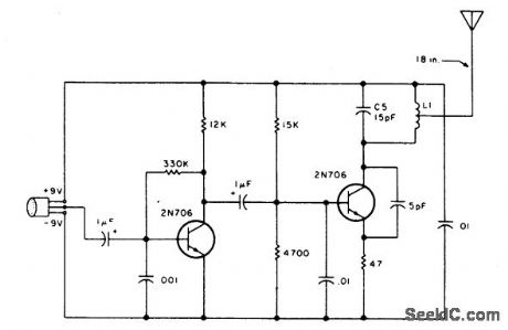
This transmitter can be tuned to the FM broadcast band, 2 meters, or other VHF bands by changing C5 and L1. The values given for C5 and L1 will place the frequency somewhere in the FM broadcast band. L1 is 4 turns of #20 enameled wire airwound, Y4 inch in diameter, 5mm long and center-tapped. The microphone is an electret type and the antenna is 18 inches of any type of wire. Keep all leads as short as possible to minimize stray capacitance. The range of the transmitter is several hundred yards. (View)
View full Circuit Diagram | Comments | Reading(0)
GROUND_FAULT_INTERRUPTER_120_Hz_NEUTRAL_TRANSFORMER_APPROACH
Published:2009/6/30 3:09:00 Author:May
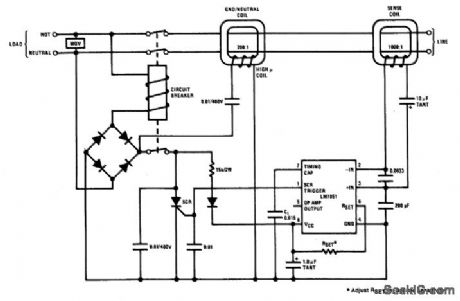
View full Circuit Diagram | Comments | Reading(598)
GROUND_TESTER
Published:2009/6/30 3:08:00 Author:May

This circuit checks the reliability of appliances so that the equipment may be used safely. The test circuit must be plugged into a properly wired three terminal wall outlet. When a two-lead or three-lead appliance is plugged into circuit outlet S01, neon lamps NE1 and NE2 will light if the appliance is safe. If neon NE2 is lit the appliance is dangerous, because the neutral lead is 110 Vac above ground. (View)
View full Circuit Diagram | Comments | Reading(887)
2_1_2_DIGIT_INPUT_FOR_199_COUNT
Published:2009/6/30 3:08:00 Author:May

Addition of 1/2-digit circuit to basic 2-digit BCD DAC increases countfrom 99 to 199,Circuit sequencesto 99 while 1/2-digitsection of MC14009 hex two-output NOR gate has low output, and goes through steps 100 to 199 while 1/2-digit output is high Reference voltage is 5.0 V. Calibration procedure is given.—T.Henry,Binary D/A Converters Can Provide BCD-Coded Conversion,EDN Magazine, Aug.5, 1973, p 70-73. (View)
View full Circuit Diagram | Comments | Reading(1012)
2_DIGIT_BCD
Published:2009/6/30 3:07:00 Author:May
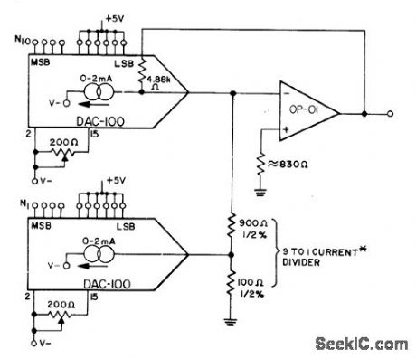
Output current of Precision Monolithics DAC-100 D/A converter can be adjusted to exactly desired value with 200-ohm pot for each DAC; adjustment is made with input of all 0s. Circuit can be expanded to 3 digits by adding third DAC and adding 99 to current divider.— 8 & 10 Bit Digital-to-Analog Converter, Precision Monolithics, Santa Clara, CA, 1977, DAC-100, p 5. (View)
View full Circuit Diagram | Comments | Reading(0)
TARRY_LIGHT
Published:2009/6/30 3:06:00 Author:May

The push button and potentiometer initiate a time delay that turns a light on then automatically turns it off again after a predetermined time. The potentiometer can be set for a delay of a few secbnds to just under three minutes. When the push-button switch SW2 is pressed, capacitor C1 gets charged through D5 to the full dc voltage developed by the diode bridge. When the button is released, the charged capacitor is connected across the series combination of R2, R3, and potentiometer R4 whose setting determines the total resistance and thereby sets the time it takes for the capacitor to discharge. A steering diode, D6, connected to the junction of R2 and R3, and potentiometer R4 whose setting determines The total resistance and thereby sets the time it takes for the capacitor to discharge. Diode, D6 picks off a portion of this decaying dc voltage and applies it to the gates terminal of Q1, the SCR, triggering it into a conductive state. This SCR will remain on as long as there is sufficient voltage on its gate. As soon as this voltage decays below the minimum holding voltage of the SCR, it will tum off on the next line alternation. (View)
View full Circuit Diagram | Comments | Reading(707)
TEMPERATURE_COMPENSATION
Published:2009/6/30 3:06:00 Author:May
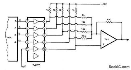
Use of 7407 hex buffer following SN7490 of D/A converter permits satisfactory performance over reasonably wide temperature range even when driving several TTL stages. Noninverting input of 741 opamp is connected to output of unused buffer at logic 0. Circuit is modification of D/A converter developed by D. James for use in simple two-digit DVM.—R. J. Chance, Improved Simple D. to A. Convener, Wireless World, Dec, 1974.p 503. (View)
View full Circuit Diagram | Comments | Reading(996)
1_A_LAMP_FLASHER_
Published:2009/6/30 3:05:00 Author:May

View full Circuit Diagram | Comments | Reading(624)
SIMPLE_DAC
Published:2009/6/30 3:05:00 Author:May

Transistors are either saturated or cut off by outputs of clock-controlled SN7490 BCD counter, Portions of emitter voltages of the four transistors are added in ratios 1:2:4:8 by 741 summing opamp to obtain analog output. Article tells how two such circuits can be combined for use in two-digit DVM.—D. James, Simple Digital to Analogue Converter, Wireless World, June 1974, p 197. (View)
View full Circuit Diagram | Comments | Reading(2265)
ONE_TUBE,10_WATT_CW_TRANSMITTER
Published:2009/6/30 3:05:00 Author:May
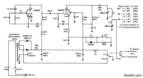
View full Circuit Diagram | Comments | Reading(1501)
RE_OSCILLATOR
Published:2009/6/30 3:05:00 Author:May

This rf oscillator is useful up to 30 MHz.An SK 3007 PNP transistor is recommended. (View)
View full Circuit Diagram | Comments | Reading(736)
| Pages:1220/2234 At 2012011202120312041205120612071208120912101211121212131214121512161217121812191220Under 20 |
Circuit Categories
power supply circuit
Amplifier Circuit
Basic Circuit
LED and Light Circuit
Sensor Circuit
Signal Processing
Electrical Equipment Circuit
Control Circuit
Remote Control Circuit
A/D-D/A Converter Circuit
Audio Circuit
Measuring and Test Circuit
Communication Circuit
Computer-Related Circuit
555 Circuit
Automotive Circuit
Repairing Circuit