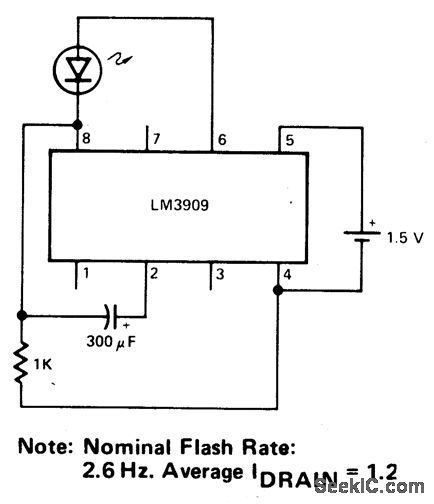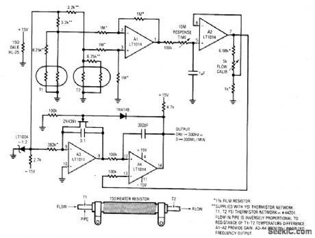
Circuit Diagram
Index 1202
PHOTOCURRENT_INTEGRATOR
Published:2009/7/1 1:44:00 Author:May
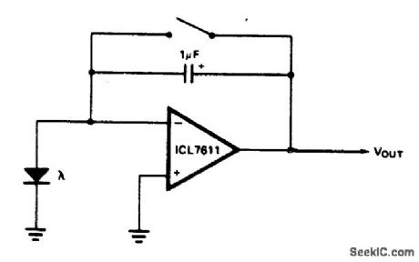
Low leakage currents allow integration times up to several hours. (View)
View full Circuit Diagram | Comments | Reading(401)
LED_BOOSTER_
Published:2009/7/1 1:44:00 Author:May
View full Circuit Diagram | Comments | Reading(631)
SYNCHRONOUS_PHOTOELECTRIC_SWITCH
Published:2009/7/1 1:43:00 Author:May

Synchronous switching is turning on only at the instant the ac supply voltage passes through zero, and turning off only when ctyrent passes through zero. This circuit provides this function in response to either a mechanical switch or a variable resistance such as a cadmium-sulfide photocell. This circuit produces the minimum disturbance to the power supply when switching, and always conducts an integral number of whole cycles. It is ideal for use wherever RFI and audio filtering is undesirable, where magnetizing inrush current of transformers causes nuisance fuse-blowing, and where sensitive equipment must operate in the vicinity of power switches. (View)
View full Circuit Diagram | Comments | Reading(999)
SAFE,HIGH_VOLTAGE_FLASHER
Published:2009/7/1 1:43:00 Author:May
View full Circuit Diagram | Comments | Reading(540)
FLASHER_FOR_4_PARALLEL_LEDs_
Published:2009/7/1 1:43:00 Author:May
View full Circuit Diagram | Comments | Reading(617)
INCANDESCENT_BULB_FLASHER
Published:2009/7/1 1:41:00 Author:May
View full Circuit Diagram | Comments | Reading(686)
LOW_FREQUENCY_DIVIDER
Published:2009/7/1 1:41:00 Author:May
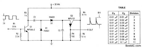
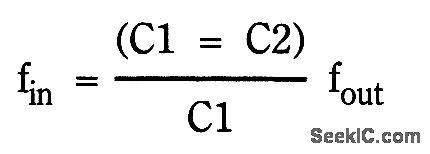

The ratio of capacitors C1 and C2 determines division. With a positive pulse applied to the base of Q1, assume that C1 = C2 and that C1 and C2 are discharged. When Q1 turns off, both C1 and C2 charge to 10 volts each through R3. On the next pulse to the base of Q1, C1 is again discharged but C2 remains charged to 10 volts. As Q1 turns off this time, C1 and C2 again charge. This time C2 charges to the peak point firing voltage of the PUT causing it to fire. This discharges capacitor C2 and allows capacitor C1 to charge to the line voltage. As soon as C2 discharges and C1 charges, the PUT turns off. The next cycle begins with another positive pulse on the base of Q1 which again discharges C1. The input and output frequency can be approximated by the equationFor a 10 kHz input frequency with an amplitude of 3 volts, the table shows the values for C1 and C2 needed to divide by 2 to 11. (View)
View full Circuit Diagram | Comments | Reading(1288)
FAST_BLINKER
Published:2009/7/1 1:40:00 Author:May
View full Circuit Diagram | Comments | Reading(421)
FREQUENCY_DOUBLER_WORKS_TO_1_MHz
Published:2009/7/1 1:37:00 Author:May
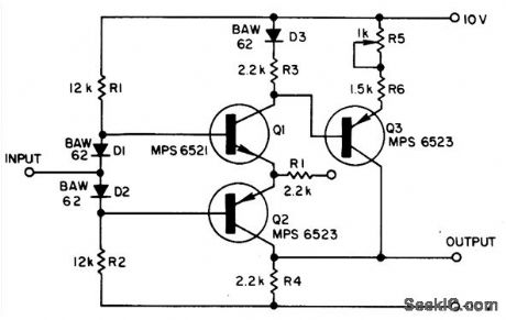
Adding components Q3, D3, and resistors R3 through R6 to a conventional complementary symmetry class AB buffer can double the frequency of an input sine wave. (View)
View full Circuit Diagram | Comments | Reading(642)
NONSELECTIVE_FREQUENCY_TRIPLER_USES_TRANSISTOR_SATURATION_CHARACTERISTICS
Published:2009/7/1 1:34:00 Author:May
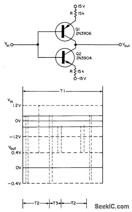
The turn-on and turn-off characteristics of two complementary transistors can be combined to attain nonselective frequency tripling. The resulting circuit handles any periodic waveform with nonvertical sides. Each input signal peak produces three output signal peaks. The additional peaks occur where the input signal causes saturation of one of the two transistors.The circuit operates over a frequency range from dc to the upper limits of the comple-mentary transistor pair. About the only disadvantage of the circuit is the lack of symmetry of the output signal peaks. (View)
View full Circuit Diagram | Comments | Reading(1122)
LOW_COST_FREQUENCY_INDICATOR
Published:2009/7/1 1:29:00 Author:May
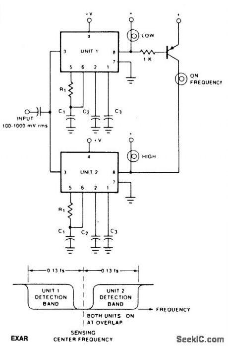
The circuit shows how two tone decoders set up with overlapping detection bands can be used for a go/no go frequency meter. Unit 1 is set 6% above the desired sensing frequency and Unit 2 is set 6% below the desired frequency.Now, if the incoming frequency is within 13% of the desired frequency, either Unit 1 or Unit 2 will give an output. If both units are on, it means that the incoming frequency is within 1% of the desired frequency. Three light bulbs and a transistor allow low cost read-out. The IC is an EXAR 567. (View)
View full Circuit Diagram | Comments | Reading(629)
POWER_FREQUENCY_METER
Published:2009/7/1 1:25:00 Author:May
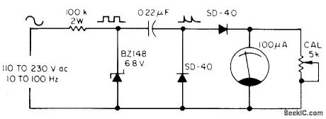
The meter uses a zener diode to form square waves from input she waves. After cal-ibration with the 5 k ohm potentiometer, the 100 μA meter reads directly in hertz. (View)
View full Circuit Diagram | Comments | Reading(1225)
TANDEM_DIMMER_CROSS_FADER
Published:2009/7/1 1:22:00 Author:May

This cross fader circuit can be used for fading between two slide projectors. As R3 is moved to either side of center, one triac is fired earlier in each half cycle, and the other later. The total light output of both lamps stays about the same for any control position. (View)
View full Circuit Diagram | Comments | Reading(1112)
LIQUID_FLOWMETER_1
Published:2009/7/1 1:21:00 Author:May
View full Circuit Diagram | Comments | Reading(464)
TRIAC_ZERO_POINT_SWITCH
Published:2009/7/1 1:21:00 Author:May

On the initial part of the positive half cycle, the voltage is changing rapidly from zero causing a large current to flow into capacitor C2. The current through C2 flows through R4, D3, and D4 into the gate of the TRIAC Q2 causing it to turn on very close to zero voltage. Once Q2 turns on, capacitor C3 charges to the peak of the line voltage through D5. When the liqe voltage passes through the peak, D5 becomes reverse-biased and C3 begins to discharge through D4 and the gate of Q2. At this time the voltage on C3 lags the line voltage. When the line voltage goes through zero there is still some charge on C3 so that when the line voltage starts negative C3 is still discharging into the gate of Q2. Thus Q2 is also turned on near zero on the negative half cycle. This operation continues for each cycle until switch 51 is closed, at which time SCR Q1 is turned on.Q1 shunts the gate current away from Q2 during each positive half cycle keeping Q2 from turning on. Q2 cannot turn on during the negative cycle because C3 cannot charge unless Q2 is on during the positive half cycle. (View)
View full Circuit Diagram | Comments | Reading(1026)
TRIAC_LAMP_DIMMER
Published:2009/7/1 1:19:00 Author:May

Using a heatsink, the TRIAC (TR1) can handle up to 350 watts. The neon lamp, I1, won't trip the gate until after it conducts and using R1, set the lighting wherever you want it. (View)
View full Circuit Diagram | Comments | Reading(0)
RUGGED_LAMP_DRIVER_IS_SHORT_CIRCUIT_PROOF
Published:2009/7/1 1:19:00 Author:May
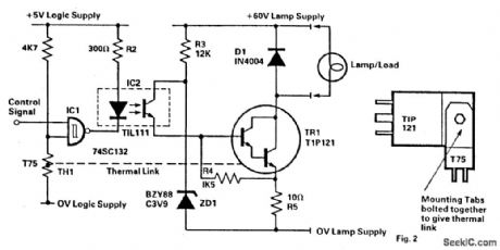
This circuit is capable of driving filament lamps of nominal rating 200 mA at 60 V dc from a CMOS logic signal.The lamp or load is connected in series with the Darlington transistor TR1 and emitter resistor R5. The Zener diode ZD1 establishes a soft reference voltage on the collector of the optical coupler IC2. When the logic control signal from the processor switches the optocoupler on via IC1, base drive is applied to TR1 and the lamp is switched on. (View)
View full Circuit Diagram | Comments | Reading(1719)
LIQUID_FLOWMETER
Published:2009/7/1 1:18:00 Author:May
View full Circuit Diagram | Comments | Reading(538)
LAMP_DIMMER
Published:2009/7/1 1:17:00 Author:May

A full range power controller suitable for lamp dimming and similar applications operate from a 120 volt, 60 Hz ac source, and can control up to 1000 watts of power to incandescent bulbs. The power to the bulbs is varied by controlling the conduction angle of TRIAC Q1. At the end of each positive half-cycle when the applied voltage drops below that of the capacitor, gate current flows out of the SBS and it switches on, discharging the capaci-tor to near zero volts. The RC network shown across the TRIAC represents a typical snubber circuit that is normally adequate to prevent line transients from accidentally firing the TRIAC. (View)
View full Circuit Diagram | Comments | Reading(1726)
PLANT_WATER_GAUGE
Published:2009/7/1 1:17:00 Author:May
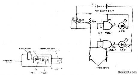
To calibrate the gauge, connect the battery and press the probes gently into a pot containing a plant that is just on the verge of needing water (stick it in so that only an inch of the probe is left visible at the top). Turn the potentiometer until the OK LED lights and then turn it back to the point where that LED goes out and the W , or Water , LED just comes on. The device should now be property adjusted. (View)
View full Circuit Diagram | Comments | Reading(566)
| Pages:1202/2234 At 2012011202120312041205120612071208120912101211121212131214121512161217121812191220Under 20 |
Circuit Categories
power supply circuit
Amplifier Circuit
Basic Circuit
LED and Light Circuit
Sensor Circuit
Signal Processing
Electrical Equipment Circuit
Control Circuit
Remote Control Circuit
A/D-D/A Converter Circuit
Audio Circuit
Measuring and Test Circuit
Communication Circuit
Computer-Related Circuit
555 Circuit
Automotive Circuit
Repairing Circuit


