About SeekIC | Services | Payment | Advertisements service | Contact Us | Links
© 2008-2012 SeekIC.com Corp.All Rights Reserved.

Published:2009/6/30 23:27:00 Author:May


This is an application of the static switch circuit where the control logic is a flip-flop which is controlled by the unijunction transistor. The flashing rate can be adjusted from about 0.1 second to a 10 second cycle time. (View)
View full Circuit Diagram | Comments | Reading(785)
Published:2009/7/24 8:20:00 Author:Jessie

This circuit is a pulse generator or astable multivibrator, where the on and off periods can be adjusted separately. The pulse rate is selected by the setting of S1, and it remains essentially constant when the on-period and off-period resistors are adjusted. Harris Semiconductor, Linear and Telecom ICs,1991, p. 3-100. (View)
View full Circuit Diagram | Comments | Reading(690)
Published:2009/6/30 23:22:00 Author:May
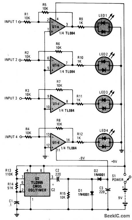


The monitoring circuit consists of four tri-color LEDs driven by an equal number of op amps configured as gain-of-one inverting amplifiers. Each LED is wired in the circuit so that it glows red when the input to the op amp is high, and green when the input is low. The LED remains off when the input is disconnected from a circuit, when it's at ground potential, and when it's connected to a 3-state output that's in the high-impedance state. Each input has an impedance of 10,000 ohms preventing the circuitfrom loading communication lines. The op amp requires both positive and negative sup-ply voltages to properly drive the LEDs. Both voltages are supplied by a single, nine-volt battery. The battery supplies the positive source directly. The negative source is supplied via a CMOS 555 oscillator/timer that's configured as an astable oscillator, which is used to drive a standard diode/capacitor voltage doubler. When the 555 is connected to the monitoring circuit, the output voltage is not 18 volts (2×9), but a little under nine volts, due to loading. The circuit draws about 16 mA with all LEDs off; with all four on, it draws between 20 and 30 mA, depending on how many LEDs are high, and how many are low. The use of CMOS op amps reduces quiescent current drain considerably. (View)
View full Circuit Diagram | Comments | Reading(701)
Published:2009/7/24 8:20:00 Author:Jessie

The advantages of a series-resonant converter, compared to a buck-derived switching regulator, are higher overall efficiency, smaller weight and volume, reduction in EMI, and increased reliability. The disadvantages are: an additional resonant circuit, the rating of the power switch is about 1.4 times higher, and the output filter capacitors must have low ESR and high ripple-current ratings. (View)
View full Circuit Diagram | Comments | Reading(1298)
Published:2009/7/24 8:19:00 Author:Jessie

This figure shows the circuit, waveforms, and characteristics, where a UJT is used as a relaxation oscillator. This basic building block is used in most of the UJT timer and control circuits (described in chapter 9). The waveforms and characteristics are shown in Figs. 5-41B and 5-41C, respectively. The waveforms are those obtained when the circuit values are: RE=10 kΩ, CE= 0.01μF, R2=200Ω, R1=47Ω, and V1=20 V. The approximate period of the oscillator pulses can be found by:RECE×1.7. The value of RE must be such that the load line (Fig. 5-41C) intersects the emitter characteristic in the negative-resistance region. Motorola Thyristor Device Data, 1991, p .1-6-37, 38. (View)
View full Circuit Diagram | Comments | Reading(1778)
Published:2009/6/30 23:17:00 Author:May

Circuit uses four LEDs to indicate direction of phase error as correct setting is approached when tuning oscillator to standard frequency. Lamps form display that rotates once per cycle at reference frequency, with brightness of each lamp being modulated at frequency of oscillator being adjusted. Dis-play thus appears to have frequency equal to difference between two signal frequencies, ro-tating in direction indicative of sense of fre-quency difference. Mount lamps on smallest possible circle. Diode and LED types are not crit-ical.-R. H. Pearson, An L.E.D. Synchroscope, Wireless World, Sept. 1974, p 321. (View)
View full Circuit Diagram | Comments | Reading(2499)
Published:2009/7/24 8:17:00 Author:Jessie

Because of their fast switching time, low-voltage hybrid circuits (such as the PIC600) can be operated as high as 250 kHz. The advantages of the higher frequencies are: lower filter cost, reduced size and weight, improved transient response, output ripple less dependent on capacitor ESR, and simpler EMI and RFI filtering. (View)
View full Circuit Diagram | Comments | Reading(1468)
Published:2009/6/30 23:17:00 Author:May

A 555 timer, IC1, drives a 4017 CM0S decade counter. Each of the 4017's first four outputs drives a CA3079 zero-voltage switch. Pin 9 of the CA3079 is used to inhibit output from pin 4, thereby disabling the string of pulses that IC normally delivers. Those pulses occur every 8,3 ms, i.e., at a rate of 120 Hz. Each pulse has a width of 120 μs.Due to the action of the CA3079, the lamps connected to the TRI-AC's turn on and off near the zero crossing of the ac waveform. Switching at that point increases lamp life by reducing the inrush of current that would happen if the lamp were turned on near the high point of the ac waveform. In addition, switching at the zero crossing reduces Radio-Frequency Interference (RFI) considerably.CAUTION: The CA3079's are driven directly from the 117-volt ac power line, so use care. (View)
View full Circuit Diagram | Comments | Reading(0)
Published:2009/7/24 8:17:00 Author:Jessie

This figure shows the circuit and corresponding waveforms, where a SIDAC is used as a relaxation oscillator. Being a negative-resistance device, the SIDAC can be used as a simple relaxation oscillator, where frequency is determined primarily by the RC time constant. Once the capacitor voltage reaches the SIDAC breakover voltage V(BO), the SIDAC fires, and dumps the charged capacitor. Power can be obtained by placing the load in the discharge path. Such a circuit can be used as an xeon flasher (Fig. 8- l4). Motorola Thyristor Device Data, 1991, p. 1-4-6. (View)
View full Circuit Diagram | Comments | Reading(1941)
Published:2009/7/24 8:15:00 Author:Jessie

This circuit shows a precision RC oscillator, where the frequency is determined by the equation 0.72/(R1C1). The circuit is particularly useful for frequencies below 3 kHz. For a bipolar ±5-V output swing, refer the ground connection to -5 V. Linear Technology Corporation, Linear Appications Handbook, 1990, p. AN20-11. (View)
View full Circuit Diagram | Comments | Reading(853)
Published:2009/7/24 8:14:00 Author:Jessie

This circuit shows an LT1011 comparator biased in the linear mode and using a crystal to establish the resonant frequency. This circuit can achieve a temperature-independent clock up to a few hundred kHz. Linear Technology Corporaton, Linear Applications Handbook, 1990, p. AN20-12. (View)
View full Circuit Diagram | Comments | Reading(720)
Published:2009/7/24 8:14:00 Author:Jessie

This circuit shows a crystal oscillator that is designed as a clock for an LTC1062 filter (chapter 7). The clock frequency is determined by the crystal and the values of C1 and C2, as shown by the table. Linear Technology Corporations Linear Applications Handbook, 1990, p. AN20-12. (View)
View full Circuit Diagram | Comments | Reading(654)
Published:2009/6/30 23:17:00 Author:May

This diagram shows a high-speed data acquisition system with 8 differential inputs and 12-bit resolution using the AM-543. If the control logic is timed so that the Sample-Hold-ADC section is converting one analog value while the mux-amplifier section is al-lowed to settle to the next input value, throughout rates greater than 156 KHz can be achieved. The AM-543 is used with Datel's ADV-817, a 12-bit hybrid A/D with a 2 μSec conversion rate, the SHM-6, a 0.01%, 1 psec hybrid Sample-Hold, and the MX-1616,a low cost, high-speed monolithic analog multiplexer. The system works as follows:The μP selects a channel and initiates a conversion at G = 1 and then looks at the MSB of the conversion result. If the MSB = 1, the μP will store the value. If the MSB = 0, the μP will select G = 2. The μP will repeat the cycle of gain incrementing, comparison, and analog-to-digital conversion until the MSB = 1. The μP will then test for an output of all 1's, as this is the full-scale output of the A/D. If the output is all 1's, the μP will decrement the gain by 1 step and perform the final conversion.
(View)
View full Circuit Diagram | Comments | Reading(1401)
Published:2009/6/30 23:16:00 Author:May

Uses transistor as driver to turn on programmable unijunction transistor (PUT) oscillator feeding 8-ohm loud-speaker. Pitch of tone can be adjusted with 10 K pot. Input is from alarm pin of digital clock IC (pin 3 for Fairchild FCM7001 equivalent of Cal-Tex CTT001}. PUT is Radio Shack 276-119 or equivalent.-W. J. Prudhomme, CT7001 Clock-buster, 73 Magazine, Dec. 1976, p 52-54 and 56-58. (View)
View full Circuit Diagram | Comments | Reading(2662)
Published:2009/6/30 23:13:00 Author:May

One CMOS transistor pair from CA3600E array is connected with feedback pinetwork to glve sta-ble oscilIator performance with 2-MHz crystal.Low power drain makes circuit ideal for use in digital clocks and watches.- Linear Integrated Circuits and MOS/FET's, RCA Solid State Divi-sion, Somerville, NJ, 1977, p 280. (View)
View full Circuit Diagram | Comments | Reading(659)
Published:2009/6/30 23:13:00 Author:May

CR1, CR2, CR3, and CR4 form a bridge circuit with the SCR across the dc legs.With light on the photoconductor PC1, C1 charges through R1 to about 150 Vdc. The resistance of PC1 is low when illuminated, so very little voltage appears across it or C2. At about 90 volts C1 starts discharging through RI and the SCR, but the SCR cannot turn off until C1 is almost completely discharged. When the SCR turns off during the interval line voltage is near zero, the full supply voltage again appears across the bridge, and C1 charges again to a high voltage. The voltage on C2 also starts rising until the neon lamp fires and the cycle repeats. An alternative remote control can be made by adding a second neon lamp, N2, and masking the photocell so it sees only N2. A very sensitive remote control is thus obtained that is completely isolated from the load circuit.For low-voltage remote control a flashlight lamp may be used instead of N2 and operated at about 1/2 its normal voltage thus giv.ing exceptionally long life. Performance of the photoelectric control may be inverted (flash when the photoconductor is illuminated) by interchanging PC1,and R2.Sensitivity in either the normal or inverted modes can be decreased by partially masking PC1, and can be increased by increasing resistor R2 to about 470 K. To increase on time, increase C1; to increase off time, increase R3. (View)
View full Circuit Diagram | Comments | Reading(538)
Published:2009/6/30 23:13:00 Author:May


Uses ordinary No.48 or 49 pilot lamp as resonance indicator will oscillate ai frequencies up to 12 MHz.Wind L1 to cover desired frequency ranges.-Circuits,73 Magazine,April 1973,p 133. (View)
View full Circuit Diagram | Comments | Reading(2578)
Published:2009/6/30 23:11:00 Author:May


A relaxation oscillator is used to flash an LED in the base circuit. C1 is charged slowly through R1 by the power source, then discharged periodically through R3 and the LED by the UJT. Flashing rate is determined by the supply voltage and by R1-C1's time constant.UJT = 2N4871 (View)
View full Circuit Diagram | Comments | Reading(2136)
Published:2009/6/30 23:04:00 Author:May
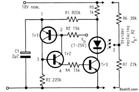
The circuit is economical in components, and will work with virtually any transistors and is reliably self-starting. The voltage Vb can be taken from a divider, as shown at the right. If taken from a fixed source, flashing becomes slower as battery voltage falls.The lowest drive current into the base of Tr3 is about (Vb-0.6 V)/(R2 + R4). Resistor R4 limits the initial current from C1 and, as shown, R2 and R4 can be roughly equal when a divider is used for Vb. Resistor R2 equals R6R7/(R6+ R7). With the voltages shown, and with R2 = R4, the on-time is about 1.1 C1R2 and the off-time about 0.28 C1R1. Using the component values shown the period is about 0.55 sec. with a duty cycle of about 7% and a mean battery current including the Vb divider, about 1.5 mA. (View)
View full Circuit Diagram | Comments | Reading(522)
Published:2009/6/30 22:58:00 Author:May


Flashing occurs each time the capacitor discharges through the tumed-on SCR. When the discharge current falls below the SCR holding current, the SCR turns off, and the capacitor begins charging for another cycle. The circuit will maintain a slower but good flashing capability even after considerable battery degradation. (View)
View full Circuit Diagram | Comments | Reading(1159)
| Pages:1211/2234 At 2012011202120312041205120612071208120912101211121212131214121512161217121812191220Under 20 |
Response in 12 hours
© 2008-2012 SeekIC.com Corp.All Rights Reserved.