
Circuit Diagram
Index 1217
VOLTAGE_TO_FREQUENCY
Published:2009/6/30 21:11:00 Author:May
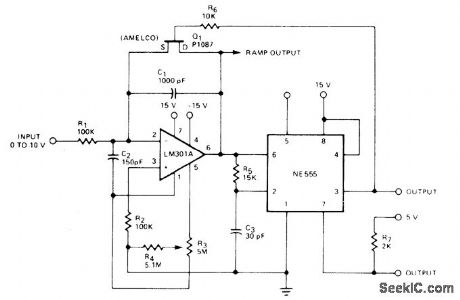
Input voltage range of 0 to -10 VDC is converted by opamp and timer to proportional frequency with good linearity. Circuitis TTL-compatible, Accuracy is 0.2%.— Signetics Analog Data Manual, Signetics, Sunnyvale, CA, 1977, p 727-729. (View)
View full Circuit Diagram | Comments | Reading(656)
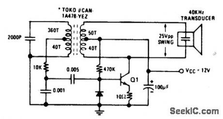
40_kHz_ULTRASONIC_TRANSMITTER_1
Published:2009/6/30 21:06:00 Author:May
View full Circuit Diagram | Comments | Reading(1080)
ULTRASONIC_PEST_REPELLER_1
Published:2009/6/30 21:05:00 Author:May
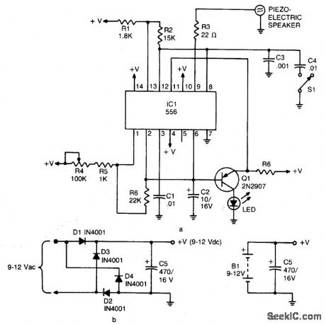
The device emits ultrasonic sound waves that sweep between 65,000 and 25,000 hertz. Designed around a 556 dual timer, one half operated as an astable )nultivibrator with an adjustable frequency of 1 to 3 Hz. The second half is also operated as an astable multivibrator but with a fixed free running frequency around 45,000 Hz. The 25-65 kHz sweep is ac-complished by coupling the voltage across C2 (the timing capacitor for the first half of the 556) via Q1 to the control voltage terminal (pin 11) of the second half of the 556. The device that radiates the ultrasonic sound is a piezo tweeter. (View)
View full Circuit Diagram | Comments | Reading(1230)
VOLTAGE_TO_FREOUENCY_GO_NO_GO
Published:2009/6/30 21:04:00 Author:May

Single UJT is used as V/F converter to provide completely isolated inputs and outputs for high-voltage go/no-go test monitor When voltage exceeds predetermined limit, output to digital frequency counter exceeds corresponding frequency limit. Output can be fed directly into digital frequency-limit detector that provides go/no-go indication.—T.H.Li,VFC Used in lsolated GO-NO GO Voltage Monitor,EDN Magazine, July 5,1974, p 75. (View)
View full Circuit Diagram | Comments | Reading(1165)
DC_VOLTAGE_TO_TIME
Published:2009/6/30 21:02:00 Author:May

Opamp connected as integrator feeds opamp comparator to produce output pulse whose width is proportional to magnitude of DC input voltage. Circuit shown is for positive inputs only; for both positive and negative inputs, article tells how to add another comparator. Circuit can then be used to generate start and stop pulses applied to digital timer of digital voltmeter.—G. B. Clayton, Experiments with Operational Amplifiers, Wireless World, Sept. 1973, p 447-448. (View)
View full Circuit Diagram | Comments | Reading(906)
HIGH_PRECISION_V_F_CONVERTER
Published:2009/6/30 21:01:00 Author:May

Active integrator using one section of RC3403A quad opamp improves linearhy, frequency offset, and response time of Raytheon RM4151 converter operating from single supply,Opamp develops null voltage,— Linear Integrated Circuit Data Book, Raytheon Semiconductor Division, Mountain View, CA, 1978, p 7-38. (View)
View full Circuit Diagram | Comments | Reading(1026)
DC_10_kHz_FREQUENCY_VOLTAGE_CONVERTER
Published:2009/6/30 5:54:00 Author:May

Circuit Notes
The converter generates an output vol-tage which is linearly proportional to the input frequency waveform. Each zero crossing at the comparator's input causes a precise amount of change to be dispensed into the op amp's sum-ming junction. This charge in turn flows through the feedback resistor generating voltage pulses at the output of the op amp.Capacitor (CINT) across Rtxt averages these pulses into a dc voltage which is linearly proportional to the input frequency. (View)
View full Circuit Diagram | Comments | Reading(1080)
3_V_FLASHER_
Published:2009/6/30 4:32:00 Author:May

View full Circuit Diagram | Comments | Reading(716)
A_D_converter_for_3_digit_LED_display
Published:2009/7/24 10:01:00 Author:Jessie

This circuit shows a CA3162A connected to a CD4511B decoder/driver to operate a common-cathode LED display. Figure 6-21B shows the PC tenmplate and component layout. The additional logic shown within the dotted area allows the display of negative numbers as low (as -99 mV), depending on the Position of the DP1/DP2 switch. The sampling rate can be changed from 4 to 96 Hz when pin 6 of'the CA3162A is connected to +5 V. To adjust, follow the proccdure described for Fig. 6-20. Harris Semiconductors, Data Acquisition, 1991, p. 2-6, 2-7. (View)
View full Circuit Diagram | Comments | Reading(2070)
LINE_OPERATED_PHOTO_ELECTRICSMOKE_ALARM_USING_LIGHT_SENSITIVE_RESISTOR(INCLUDESDETEC_TION_OF_OPEN_CIRCUITED_LED)
Published:2009/6/30 3:51:00 Author:May

View full Circuit Diagram | Comments | Reading(760)
A_D_converter_for_3_digit_LCD_display
Published:2009/7/24 9:57:00 Author:Jessie
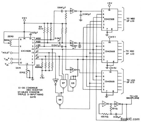
This circuit shows a CA3162E and three CD4056B LCD decoder/drivers connected in a typical LCD application. With pin 6 of the CA3162E floating (as shown), the sampling rate is 4 Hz. The negative sign (-) is decoded as a negative sign (-), and the positive overload indicator (E) as an H . To adjust, short terminals 10 and 11 of the CA3162E, and adjust the zero control for a reading of 000 on the display. Then, apply 900 mV at terminals 10 and 11, and adjust the gain control for a reading of 900 on the display. Harris Semiconductors, Data Acquisition, 1991, p. 2-5. (View)
View full Circuit Diagram | Comments | Reading(2021)
19_V_BATTERY_OPERATEDIONIZATION_TYPE_SMOKEDETECTOR
Published:2009/6/30 3:49:00 Author:May

View full Circuit Diagram | Comments | Reading(575)
Interfacing_D_A_converters_with_digital_logic_families
Published:2009/7/24 9:54:00 Author:Jessie

This circuit shows the interface circuits that are required to interface a typical TTL DAC with ECL,CMOS, PMOS, and NMOS digital devices. Raytheon Linear Integrated Circuits, 1989, p. 6-15. (View)
View full Circuit Diagram | Comments | Reading(907)
Differential_line_driver_to_drive_an_ARINC_429_bus
Published:2009/7/24 9:52:00 Author:Jessie
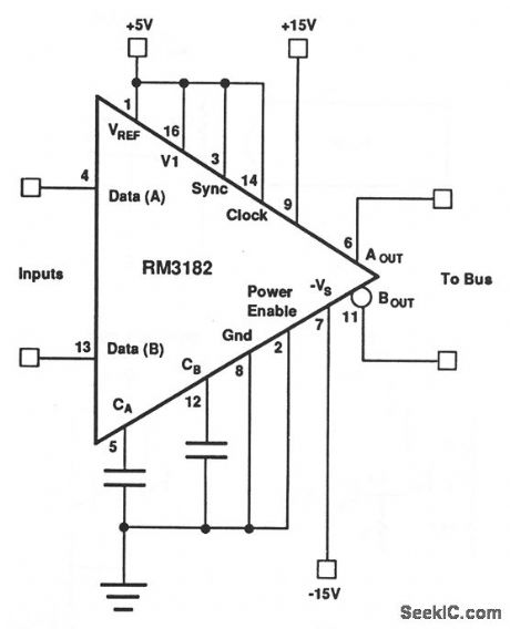
With this circuit, the output impedance is 75Ω. When data-A is high and data-B is low, AOUT swings to +VREF and BOUT swings to -VREF, and vice versa. The slew rate is set by CA/CB. Typical values are 15 pF for 100 Kb/s and 500pF for 12.5 to 14 Kb/s. Raytheon Linear Integrated Circuits, 1989, p. 11-6. (View)
View full Circuit Diagram | Comments | Reading(718)
PHOTOELECTRIC_SMOKE_DETECTOR_NON-LATCHING
Published:2009/6/30 3:48:00 Author:May
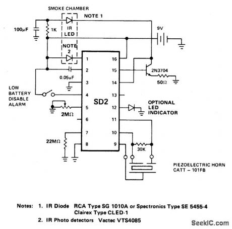
The LED predriver output pulses an ex-temal transistor which in turn, switches on the infrared light emitting diode at a very low duty cycle. The desired IR LED pulse period is determined by the value of the external timing resistor. The Smoke Sensitivity is adjustable through a trimmer resistor which varies the IR LED pulse width. The light sensing element is a silicon photovoltaic cell which is held at near zero bias to minimize leakage currents. The circuit can detect signals as low as 1 mV and generate an alarm. The IR LED pulse repetition rate increases when smoke is detected. (View)
View full Circuit Diagram | Comments | Reading(753)
A_D_converter_with_latch
Published:2009/7/24 9:49:00 Author:Jessie
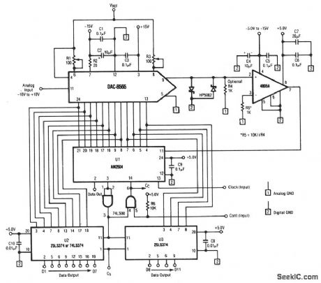
This circuit shows a DAC and comparator that is used with an SAR form a 12-bit A/D converte. Latched output is provided by the 25LS374.The reference is set by R1 and the bipolar offset is controlled by R3. Raytheon Linear Integrated Circuits, 1989, p. 6-96. (View)
View full Circuit Diagram | Comments | Reading(1101)
SCHMITT_TRIGGER
Published:2009/6/30 3:46:00 Author:May

The lower trigger point is fixed at 1/3 Vcc, but the upper trigger point is adjustable by means of Pin 5 from 1/3 Vcc to slightly less than Vcc. The Schmitt triggerwill operate with input frequencies up to 50 kHz. (View)
View full Circuit Diagram | Comments | Reading(3405)
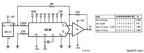
A_D_converter
Published:2009/7/24 9:46:00 Author:Jessie
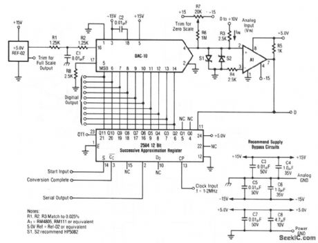
This circuit shows a DAC and comparator that is used with a 12-bit SAR to form a 10-bit A/D converter. The analog input (0 to + 10 V) is applied at R3. Both parallel and serial digital outputs are available. R7 is used to trim for zero. Full-scale is trimmed by REF-02 (Fig. 4-1C). Raytheon Linear Integrated Circuits, 1989, p. 6-28. (View)
View full Circuit Diagram | Comments | Reading(1964)
SCHMITT_TRIGGER_ZERO_CROSSING_DETECTOR_WITH_HYSTERESIS
Published:2009/6/30 3:46:00 Author:May
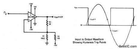
This circuit has a 100 mV hysteresis which can be used in applications where very fast transition times are required at the output even though the signal is very slow. The hysteresis loop also reduces false triggering due to noise on the input. The waveforms show the trip points developed by the hysteresis loop. (View)
View full Circuit Diagram | Comments | Reading(1109)
Offset_binary_D_A_converter_operation
Published:2009/7/24 9:42:00 Author:Jessie
This circuit shows a DAC/op-amp combination that is used to provide offset-binary operation. Raytheon Linear Integrated Circuits, 1989, p. 6-14. (View)
View full Circuit Diagram | Comments | Reading(1)
| Pages:1217/2234 At 2012011202120312041205120612071208120912101211121212131214121512161217121812191220Under 20 |
Circuit Categories
power supply circuit
Amplifier Circuit
Basic Circuit
LED and Light Circuit
Sensor Circuit
Signal Processing
Electrical Equipment Circuit
Control Circuit
Remote Control Circuit
A/D-D/A Converter Circuit
Audio Circuit
Measuring and Test Circuit
Communication Circuit
Computer-Related Circuit
555 Circuit
Automotive Circuit
Repairing Circuit