
Circuit Diagram
Index 1026
MUSIC_ON_HOLD
Published:2009/7/6 20:29:00 Author:May

With this music-on-hold device, you can answer the phone in one room, place the caller on hold, and then pick up the phone again at another location. When you pick up the phone the second time, you automatically deactivate the music-on-hold feature and can continue your conversation. (View)
View full Circuit Diagram | Comments | Reading(1803)
SLOW_STEPPER
Published:2009/7/6 20:28:00 Author:May
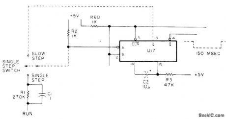
Addition of slow-stepping switch position to single-step circuit of micro.processor eliminates need for pushing single step switch repeatedly while executing endless loop program and watching address and data lights to see where program or hardware fails during debugging run. Circuit uses 74123 mono MVBR to give 1,5-ms pulses on single step and 150-ms on slow step.-H. R. Bendrot, The Slow-Stepping Debugger, Kilobaud, April 1977, p 60. (View)
View full Circuit Diagram | Comments | Reading(1070)
TELEPHONE_RINGING_DETECTORFREQUENCY_AND_VOLUME_CONTROLLED
Published:2009/7/6 20:28:00 Author:May

With the 555 timer connected as a multivibrator and an opto-isolator, a remote speaker can be driven. (View)
View full Circuit Diagram | Comments | Reading(720)
AUTOMATIC_TELEPHONE_RECORDING_DEVICE
Published:2009/7/6 20:27:00 Author:May

The device is a dc switch that is normally on via the forward biasing of Q1 via R3.Q1 now clamps Q2 into a forward state by biasing its complement well into a saturated state via R4. The dc switch is turned off via a negative voltage above that of the zener (D1). This voltage is usually about 48 and is the on-hook value of the phone line. This negative voltage overrides the effect of R3 and keeps the circuit off. When the phone is off the hook, the 48 vblts drops to 10 volts, that is below the zener voltage of D1 and R3 now tums the circuit on. The audio signal is via attenuator resistor R1 and dc isolating capacitors C1, C2. The device is a high impedance switch that isolates the recording controlled device from the phone line via some relatively simple electronic circuitry. It requires no battery and obtains power for operating via the remote jack that in most recorders is a source of 6 volts. When clamped to ground it initiates recorder operation. The unit interfaces with most portable cassette recorders providing they contain a remote control jack.
(View)
View full Circuit Diagram | Comments | Reading(757)
LIGHT_PEN
Published:2009/7/6 20:26:00 Author:May
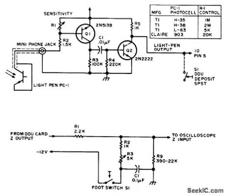
Photocell in tip of light pen senses when dot is written on screen at its location by becoming conductive and biasing al so it feeds short pulse through 01 to base of 02. If pulse is greater than 0.6V, Q2 is driven into saturation and output of pen drops to 0.3 V. Output line goes to pin 5 of digital display unit (DDU), which writes 1 or 0 (dot or no dot! on screen at instant that electron beam of CRT terminal reaches position of pen. Sensitivity control can be adjusted so illuminated dot just ahead of pen can be used to create new dot in adjacent dark space. If screen is dark all around pen, footswitch-con-trolled auxiliary circuit can be used to override Z-axis control and flood screen with light momentarily by feeding logic 1 to2 input. This mode can be used for creating or correcting graphics.-S. S. Loomis, Let There Be Light Pens, BYTE, Jan, 1976, p 26-30. (View)
View full Circuit Diagram | Comments | Reading(924)
DUAL_TONE_DECODING
Published:2009/7/6 20:26:00 Author:May

Two integrated tone decoders, XR-567 units, can be connected (as shown in Fig.1A) to permit decoding of simultaneous or sequential tones. Both units must be on before an output is given. RIC1 and R'1C'1 are chosen, respectively, for Tones 1 and 2. If sequential tones (1 followed by 2) are to be decoded, then C3 is made very large to delay turn-off of Unit Luntil Unit 2 has turned on and the NOR gate is activated. Note that the wrong sequence (2 followed by 1) will not provide an output since Unit 2 will turn off before Unit 1 comes on. Figure 1B shows a circuit variation which eliminates the NOR gate. The output is taken from Unit 2, but the Unit 2 output stage is biased off by R2 and CR1 until activated by Tone 1. A further variation js given in Fig. IC.Here, Unit 2 is turned on by the Unit 1 output wh.en Tone 1 appears, reducing the standby power to half. Thus, when Unit 2 is on, Tone 1 is or was present. If Tone 2 is now present, Unit 2 comes on also and an output is given. Since a transient output pulse may appear at Unit 1 turn-on, even if Tone 2 is not present, the load must be slow in response to avoid a false output due to Tone 1 alone. The XR-267 Dual Tone Decoder can replace two integrated tone decoders in this application.
(View)
View full Circuit Diagram | Comments | Reading(711)
MUSICAL_TELEPHONE_RINGER
Published:2009/7/6 20:24:00 Author:May

The heart of the circuit is IC1, General Instrument's AY-3-1350 melody-synthesizer IC. IC2 is a TCM1512 telephone ring detector IC that is powered by the telephone line. The circuit's operation begins when IC2 senses a ring pulse on the telephone line. The detector (internally) rectifies the ring signal and then outputs a voltage to relay RY1 (an SPST reed-type relay with 5 volt contacts), causing its contacts to close. That pulls pin 12 (the ON/OFF control) of IC1 low (logic 0 ), causing it to output a signal-the selected tune-to transistor amplifier Q2. The amplified signal is then fed to the speaker. The melody continues to play either until the tune is finished (at which time IC1 returns to the standby mode), or until someone takes the phone off the hook. Taking the phone off the hook dis-continues the ring pulses to IC2, which opens RY1. When the relay contacts open, pin 12 of IC1 goes high, returning the circuit to the standby mode to wait for the next incoming phone call. (View)
View full Circuit Diagram | Comments | Reading(3338)
FREQUENCY_TO_VOLTAGE_CONVERTER
Published:2009/7/6 20:23:00 Author:May

Six components can configure a circuit whose output voltage is proportional to its input frequency. The average current VAVG from the 40106 Schmitt trigger inverter's ground pin 8 is linearly dependent on the frequency at which C0 is discharged into the op amp's summing junction. The op amp forces this current to flow through the 13.33-KΩ feedback resistor, producing a corresponding voltage drop. This frequency-to-voltage converter yields 0 to -10 V output with 0 to 10 kHz input frequencies. (View)
View full Circuit Diagram | Comments | Reading(0)
TERMINAL_INTERFACE
Published:2009/7/6 20:22:00 Author:May
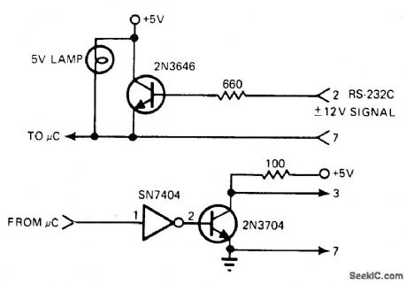
Developed for use between computer terminal and microprocessor development board. Provides interface between teleprinter terminal using EIA RS-2320 standard and input of microcomputer (upper diagram) and interface bemoan computer and teleprinter using 20-mA current-loop standard for actuating printout. Logic 1 is -3 to -9 V or less, and logic 0 is +3 to +9 V or more.-P. Snigier, Constructing a Low-Cost Terminal Inter-face, EDN Magazine, June 5, 1977, p 205-206. (View)
View full Circuit Diagram | Comments | Reading(610)
SINGLE_CHIP_FREQUENCY_DOUBLER
Published:2009/7/6 20:21:00 Author:May
The frequency doubler uses only one IC. Like other doublers, this circuit uses both the rising and falling edges of the input signals to produce digital pulses, thus effectively doubling the input's frequency.Without the rc networks at IC1 inputs, IC1 would not produce any output pulses. However, the rc networks delay one edge with respect to the other. The A input lags the B input for positive-going edges, and the B input lags the A input for negative-going ones. You can vary the output duty cycle from 0 to 100% by varying R3. IC1's minimum output pulse width defines the maximum frequency of this circuit. (View)
View full Circuit Diagram | Comments | Reading(1602)
SCRAMBLE_PHONE
Published:2009/7/6 20:21:00 Author:May
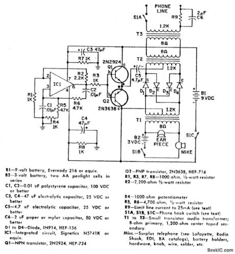
IC-1 and the associated circuitry form a stable audio tone generator that feeds a buffer amplifier, Q1 and Q2. The tone output is taken from the emitters of the transistor pair to supply a carrier voltage for a balanced modulator made up of four diodes-Dl through D4-and T1 and T2. If the two transformers and the four diodes are perfectly matched (which is almost impossible to achieve and not necessary in any case) no carrier will appear at the input or output of T1 or T2. In a practical circuit, a small amount of unbalance will occur and produce a low-level carrier tone at the input and output of the balanced modulator. A telephone carbon mike and earpiece are connected to the low impedance winding of T1, with a three volt battery supplying the necessary mike current.Trim potentiometer R4 is used to make a fine frequency adjustment of the oscillator so that two scrambler units may be synchronized to the same carrier frequency. Rg limits,line current to 25 mA. (View)
View full Circuit Diagram | Comments | Reading(717)
ODD_NUMBER_COUNTER_DIVIDER
Published:2009/7/6 20:20:00 Author:May
This circuit, shown symmetrically, divides an input by virtually any odd number. The circuit counts n + 1/2 clocks twice to achieve the desired divisor. By selecting the proper n, which is the decoded output of the LS161 counter, you can obtain divisors front 3 to 31. The circuit, as shown, divides by 25; you can obtain higher divisors by cascading additional LS161 counters. The counter and IC5A form the n + 1/2 counter. Once the counter reaches the decoded count, n, IC5A ticks off an additional 1/2 clock, which clears the counter and puts it in hold. Additionally, IC5A clocks IC5B, which changes the clock phasing through the XOR gate, IC1. The next edge of the input clocks IC5A, which reenables the counter to start counting for an additional n + 1/2 cycles. Although the circuit has been tested at 16 MHz, a worst-case timing analysis reveals that the maximum input frequency is between 7 and 8 MHz. (View)
View full Circuit Diagram | Comments | Reading(834)
SPEECH_ACTIVITY_DETECTOR_FOR_TELEPHONE_LINES
Published:2009/7/6 20:19:00 Author:May

The circuit can be used in telephone lines for speech activity detection purposes.This detection is very useful in the case of half-duplex conversation between two stations, in the case of simultaneous transmission of voice and data over the same pair of cables by the method of interspersion data on voice traffic, and also in echo suppressor devices.The circuit consists of a class-A amplifier in order to amplify the weak analog signals (in the range 25-2100 mW of an analog telephone line).The IC1 is connected as a retriggerable monostable multivibrator with the Tr2 discharging the timing capacitor C3, if the pulse train reaches the trigger input 2 of IC1 with period less than the time:
Thigh=1.1 (R3 C3)
The output 3 of IC1 is active ON when an analog or digital signal is presented at the output and it drops to low level, Thigh seconds after the input signal has ceased to exist. (View)
View full Circuit Diagram | Comments | Reading(642)
DIVIDE_BY_1_1_2_CIRCUIT
Published:2009/7/6 20:18:00 Author:May


An input signal drives both SN7474 D-type flip-flops, which are positive edge-triggered devices. A low-to-high input signal transition triggers the A flip-flop, while a high-to-low input signal transition triggers the B flip-flop via the SN7404 inverter. Either flip-flop in the high state will cause the output to decrease via the SN7402 NOR gate. This in turn disables the opposite flip-flop from going to the high state. The flip-flop in the high state remains there for one clock period, then it is clocked low. With both flip-flops low, the output increases, enabling the opposite flip-flop to be clocked high one-half clock cycle later. This alternate enabling and disabling action of the flip-flops results in a divide-by-1 1/2 function. That is, three clock pulses in, produce two evenly spaced clock pulses out. The circuit has no lock-up states and no inherent glitches. Replacing the NOR gate with an SN7400 NAND gate inverts the A, B, and output signals. By adding sim-ple binary or BCD counters, counting chains, such as divide-by-3, -6, -12, -24, -15, -30, etc., can be gen-erated using the divide-by-1 1/2 circuit as a basis. (View)
View full Circuit Diagram | Comments | Reading(2593)
POT_INTERFACE
Published:2009/7/6 20:18:00 Author:May
Circuit converts resistance of pot setting to frequency with NE555 timer IC1.Frequency is measured under direct control of microprocessor program, using 8-bit counter with CPU clock as time base. Processor is programmed to clear counter, turn on counter, wait 2 ms, turn off counter, and read count. Result is number of cycles in 2-ms period, ranging from 1 to about 240. Relationship of frequency to control position is accurate enough for game control. R1, R2, R3, and 01 are chosen so frequency varies from about 0.75 to 122 kHz as Ra is varied from 100K to 0. Use audio-taper pot to improve conversion linearity. Article gives subroutines for Motorola 6800 and Intel 8080 microprocessors.-C. Helmers, Getting Inputs from Joy-sticks and Slide Pots, BYTE, Feb. 1976, p 86-88. (View)
View full Circuit Diagram | Comments | Reading(1840)
TAPE_RECORDER_POSITION_INDICATOR_CONTROLLER
Published:2009/7/6 20:16:00 Author:May
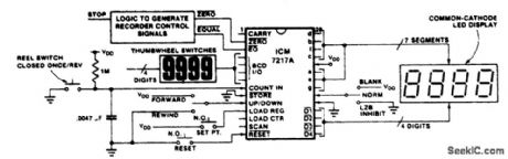
This circuit is representative of the many applications of up/down counting in monitoring dimensional position. In the tape recorder application, the LOAD REGIS-TER, EQUAL, and ZERO outputs are used to control the recorder. To make the recorder stop at a particular point on the tape, the register can be set with the stop at a particular point on the tape, the register can be set with the stop point and the EQUAL output used to stop the recorder either on fast forward, play or rewind.To make the recorder stop before the tape comes free of the reel on rewind, a leader should be used. Resetting the counter at the starting point of the tape, a few feet from the end of the leader, allows the ZER0 output to be used to stop the recorder on rewind, leaving the leader on the reel. The 1 M ohm resistor and.0047 μF capacitor on the COUNT INPUT provide a time constant of about 5 ms to debounce the reel switch.The Schmitt trigger on the COUNT INPUT of the ICM7217 squares up the signal before applying it to the counter. This technique may be used to debounce switchclosure inputs in other applications. (View)
View full Circuit Diagram | Comments | Reading(589)
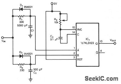
DIGITAL_FREQUENCY_DOUBLER
Published:2009/7/6 20:15:00 Author:May
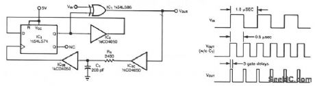
The circuit doubles the frequency of a digital signal by operating on both signal edges. Each transition causes exclusive-OR gate IC1 to produce a pulse, which clocks flip-flop IC3 after propagating through buffers IC2C and IC2B. If you remove capacitor C1, the circuit produces narrow output pulses. By including C1, you can obtain a desired duty cycle for a given input frequency flN. The C1 value for an approximate 50% dutycycle is: (View)
View full Circuit Diagram | Comments | Reading(1401)
PCF8596 Microcomputer and Auxiliary Function Integrated Circuit
Published:2011/7/29 0:01:00 Author:Michel | Keyword: Microcomputer, Auxiliary Function, Integrated Circuit

PCF8596 is PCF8596 microcomputer and the auxiliary function integrated circuit produced by Philips Company and it is widely used in ChangHong series color TVs.
First,Functions Features
Inside Assitant Circuit of PCF8596 Integrated CircuitPCF859 IC adopts 8 feet DIP package and its pins functions and data are shown as table 1 and the data is measured from ChangHong CN-15 big screen color TV.
Table 1:PCF8596 IC Pins Fuctions and Data (View)
View full Circuit Diagram | Comments | Reading(649)
TAPE_RECORDER_INTERFACE
Published:2009/7/6 20:12:00 Author:May
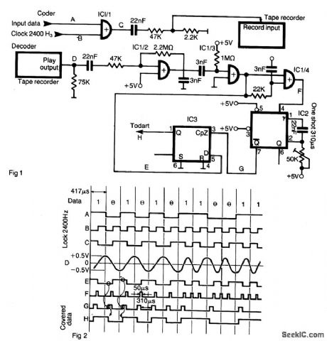
The interface allows data to be saved on an ordinary tape recorder at a speed of 2400 bit/s.The serial stream of data Fig. 1 (A) is coded with a clock of 2400 Hz (B), by means of XOR gate IC 1/1. Logical high and low appear as shown in Fig. 2 (C). These impulses are lowered in amplitude and feed into the record input of a low cost tape recorder.During the playback, pulses (D) are amplified with CMOS gate IC 1/2 connected as a linear amplifier, and providing a TTL level signal shown in (E). On both positive and negative transitions IC 1/4 forms short pulses as shown in (F) (approx. 50 ps) that triggers one shot IC2. A monostable one shot pulse width is adjusted to be 3/4 of bit length (310 pts). A change from high to low in a coded stream generates a low pulse width of one bit cell. The same is for change from low to high that generates a high pulse of the same width. During this pulse one shot latches the state of line E in D type flip-flop IC3 (G). When a stream consists of multiple ones or zeros, the one shot is retriggered before it comes to the end of the quasistable state and the state of the flip-flop remains unchanged. The original data stream is available at the output of the flip-flop (H). 280 the DUART that receives these pulses is programmed so that the receiver clock is 16 times the data rate (38.4 kHz). (View)
View full Circuit Diagram | Comments | Reading(746)
AC_STATIC_SPDT_SWITCH
Published:2009/7/6 20:11:00 Author:May
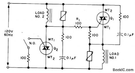
An SPDT solid state relay is shown. When voltage is applied Q1 will tum on, activating load #1, because the full line voltage appears across Q2, supplying gate current through R1. When S1 is closed, Q2 turns on removing the gate drive from Q1 and activating load #2. (View)
View full Circuit Diagram | Comments | Reading(819)
| Pages:1026/2234 At 2010211022102310241025102610271028102910301031103210331034103510361037103810391040Under 20 |
Circuit Categories
power supply circuit
Amplifier Circuit
Basic Circuit
LED and Light Circuit
Sensor Circuit
Signal Processing
Electrical Equipment Circuit
Control Circuit
Remote Control Circuit
A/D-D/A Converter Circuit
Audio Circuit
Measuring and Test Circuit
Communication Circuit
Computer-Related Circuit
555 Circuit
Automotive Circuit
Repairing Circuit