
Circuit Diagram
Index 1038
Video_amplifier_dc_stabilizer_differentially_sensed_technique
Published:2009/7/22 22:21:00 Author:Jessie
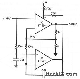
In this circuit, sensing is done differentially, preserving access to both fast amplifier inputs. A1 measures the dc error at the A2 input, and biases the offset pins to force offset within 50 μV. The offset-pin biasing at A2 is arranged so that A1 is always able to find the servo point. The 0.01-μF capacitors rolls off Al at the low frequency, and A2 handles the high-frequency signals. The combined characteristics yield: gain-bandwidth of 45 MHz, offset voltage of 50 μV, offset drift of 1 μV/℃, and a slew rate of 250 V/μs.
(View)
View full Circuit Diagram | Comments | Reading(613)
Optically_controlled_regulator_shutdown
Published:2009/7/22 22:20:00 Author:Jessie
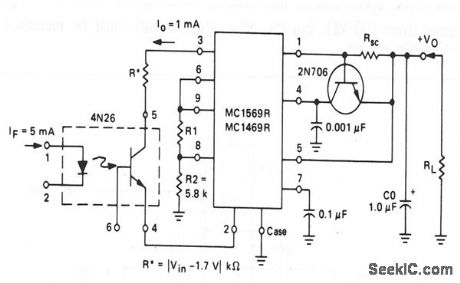
This circuit shows a 4N26 that is used to shut down a voltage regulator. To ensure that the regulator is shut down, input current to the 4N26 LED must be a minimum of 5 mA (to produce 1 mA at thq 4N26 output). (View)
View full Circuit Diagram | Comments | Reading(1542)
WAVEFORM_TESTER
Published:2009/7/22 22:20:00 Author:Jessie
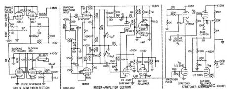
Used in high-speed testing of ferrite cores, transistors, transformers, and other components requiring waveform measurement. Based on sampling of un known waveform at discrete intervals and comparing resulting digital output with that provided by perfect component.-B. Agusta, Sorting Components by Measuring Waveforms, Electronics, 32:7, p 56-59. (View)
View full Circuit Diagram | Comments | Reading(651)
P87C766 Single-chip Microcomputer Integrated Circuit
Published:2011/7/28 22:12:00 Author:Michel | Keyword: Single-chip, Microcomputer, Integrated Circuit
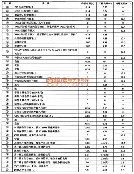
P87C766 is single-chip microcomputer integrated circuit produced by Phlips Company and it is special main control chip of ChangHong DT2000 frequency doubling color TV electric set.
First,Function Features P87C766 contains the CPU (central processing unit), the I2C bus circuit, OSD showing circuit, all kinds of identification signal circuit, all sorts of function control circuit, and some other auxiliary functions circuit.
Second,Pins Functions and Data
P87C766 IC adopts feet 42 DI{ package and P87C766 on DT2000 color TV and its pins functions and data are shown as table 1.The voltage of the table, change means that it is in unstable condition when the voltage is measured.
(View)
View full Circuit Diagram | Comments | Reading(537)
Optically_coupled_RS_flip_flop
Published:2009/7/22 22:16:00 Author:Jessie
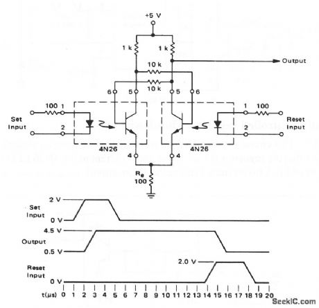
This circuit uses two 4N26 couplers to form an RS circuit with two stable states. A +2-V signal at the set input changes the output from low to high, and a +2-V signal at the reset input returns the output to low. The input pulse width must be 3 μs (minimum). (View)
View full Circuit Diagram | Comments | Reading(806)
RESISTANCE_CHECKER
Published:2009/7/22 22:15:00 Author:Jessie
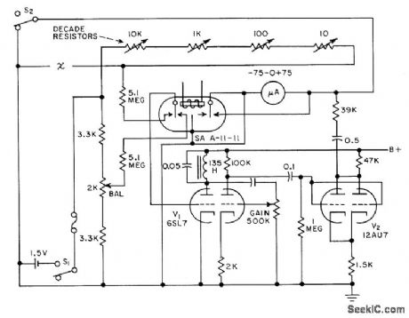
Amplified error voltage from Wheatstone bridge feeds 75-0-75 microammeter to indicate whether resistance under test is higher or lower than desired value und within preset tolerance. Instrument range is 9,999 ohms in 1-ohm steps. Gives go-no-go indication, to speed production testing.-D. S. Randall, Go No-Go Meter Speeds Resistance Check, Electronics, 31;9, p 66-68. (View)
View full Circuit Diagram | Comments | Reading(658)
FEED_FORWARD_OPAMP
Published:2009/7/6 6:51:00 Author:May
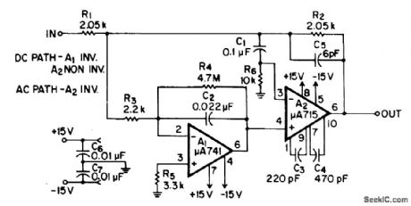
DC input characteristics are determined by A1, which is bypassed at high frequencies, while AC-coupled A2 deter-mines dynamic performance. Resulting composite amplifier combines such desired properties as low input current and drift, large bandwidth and slew rate, and fast settling time. Compensation network C3-C4-C5 is chosen first to give desired bandwidth. Composite rolloff of 6 dB per octave is then obtained by narrow-banding A1 with R4 and C2, so gain-bandwidth product is equal to ratio between unity-gain crossover frequency of A2 and open-loop gain.-Fairchild Linear IC Contest Winners, EEE Magazine, Jan. 1971, p 48-49. (View)
View full Circuit Diagram | Comments | Reading(840)
CAPACITANCE_MU_LTIPLIER
Published:2009/7/6 6:49:00 Author:May
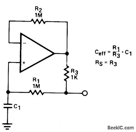
Resistance ratio determines factor by which value of C1 is multiplied when used in simple opamp circuit shown. With values shown, ratio is 1000 and 10-μF capacitor provides effective capacitance of 10,000μF. Q of circuit is limited by effective series resistance, so R1 should be as large as practical. Opamp type is not critical- Signetics Analog Data Manual, Signetics, Sunnyvale, CA, 1977, p 640-641. (View)
View full Circuit Diagram | Comments | Reading(549)
MINIMIZING_PHASE_ERROR
Published:2009/7/6 6:48:00 Author:May
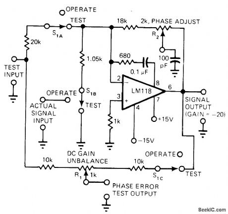
Phase compensation circuit trimmed by R2 keeps phase error of LM118 opamp well below 1° from DC to 200 kHz. In-phase error due to gain peaking is also low. Feed-forward network connected to pin 8 improves stability, making feedback capacitor unnecessary. Step response has about 30% overshoot, and sine response has about +1 dB of peaking before going 3 dB down at about 2 MHz.-R. A. Pease, Technique Trims Op-Amp Amplifiers for Low Phase Shift, EDN Magazine, Aug.20,1977, p 138. (View)
View full Circuit Diagram | Comments | Reading(550)
Minimum_component_phono_amp
Published:2009/7/22 22:11:00 Author:Jessie

This circuit shows an LM380 power-amplifier IC used as a phono amplifier The circuit has a voltage-divider volume control, with high-frequency rolloff tone control, and provides about 2.5 W to an 8-Ω speaker. (View)
View full Circuit Diagram | Comments | Reading(1829)
SINGLE_ENDED_JFET
Published:2009/7/6 6:47:00 Author:May
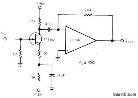
Basic JFET amplifier is virtually free from popcorn noise problems of bipolar transistors and bipolar-input opamps. Combining JFET transconductance amplifier with current-to-voltage opamp adds high voltage gain and simplifies circuit applications. Gain-limiting 7.5K FET drain resistor is by passed and removed from gain equation. Parameter variation problems are minimized by biasing FET source through 15.1K resistance to negative supply. Gain variations are minimized by leaving 100 ohms of this resistance unby-passed.-L. Maxwell, FET Amplifiers-Take Another Look at These Devices, EDN Magazine, Sept. S, 1977, p 161-163. (View)
View full Circuit Diagram | Comments | Reading(2185)
SIGN_CHANGER
Published:2009/7/6 6:46:00 Author:May
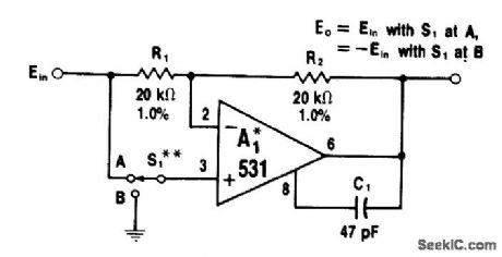
When switch S1 grounds pin 3 of opamp, circuit becomes inverter providing 180° phase shift. When S1 is at position A, input voltage acts on both inputs of A1 and no current flows through R1 and R2; output voltage is then equal to input voltage. Switch permits remote programming of phase reversal. For higher input impedance, 1556 opamp can be used.-W. G. Jung, IC Op-Amp Cookbook, Howard W. Sams, Indianapolis, IN, 1974, p 208-209. (View)
View full Circuit Diagram | Comments | Reading(711)
ABSOLUTE_VALUE_RECTIFIER
Published:2009/7/6 6:46:00 Author:May

Use of CA3140 bipolar MOS opamp in inverting gain configuration give symmetrical full-wave output when equality of design equations is satisfied. Bandwith for -3 dB is 290 kHz, and average DC output is 3.2V for 20V p-p input.- Circuit Ideas for RCA linear ICs, RCA Solid State Division, Somerville, NJ, 1977, p 18. (View)
View full Circuit Diagram | Comments | Reading(1019)
DEAD_BAND_RESFONSE
Published:2009/7/6 6:45:00 Author:May

With bridge in feed-back loop of opamp, low-level input signals give essentially 100% feedback around A1 so there is very little output voltage. When input current through R1 rises above allowable current limit of circuit, bridge opens and output voltage jumps to new level determined by R2. Input is then amplified by ratio of R2/R1 in normal linear manner. Circuit thus has dead-band property for low levels. Value of R1 sets threshold level.-W. G. Jung, IC Op-Amp Cookbook, Howard W. Sams, Indianapolis, IN, 1974, p 206-207. (View)
View full Circuit Diagram | Comments | Reading(1006)
SUMMING_WITHOUT_ADJUSTMENTS
Published:2009/7/6 6:44:00 Author:May
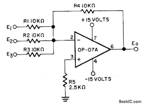
Single-stage opamp for analog computation provides high-precision output that is function of multiple input variables. Circuit drift is less than 2μV per month, eliminating need for periodic calibration while ensuring long-term accuracy. Opamp is Precision Monolithics op-07A.-D. Soderquist and G. Erdi, The op-07 Ultra-Low Offset voltage op Amp-a Bipolar Op Amp. That Challenges Choppers, Eliminates Nulling, Precision Monolithics, Santa Clara, CA, 1975, AN-13, p 11. (View)
View full Circuit Diagram | Comments | Reading(665)
3_W_PULSE_AMPLIFIER
Published:2009/7/6 6:43:00 Author:May
Motorola MC1554 power amplifier provides voltage gain of 18 for peak pulse power output up to 3 W Maximum peak output current rating of 500 mA for IC should not be exceeded during peak of output pulse.- The MC1554 One-Watt Monolithic Integrated Circuit Power Amplifier, Motorola, Phoenix, AZ, 1972, AN-401, p 3. (View)
View full Circuit Diagram | Comments | Reading(858)
PRECISE_RECTIFICATION
Published:2009/7/6 6:42:00 Author:May
Use of opamp in combination with silicon diode overcomes nonlinearity of diode at forward voltages under about 0.5 V. Offset-voltage pot is adjusted for symmetrical output waveform for small input voltages. D1 is connected in opamp feedback path so initial forward voltage drop required to make diode conduct is supplied by amplifier output. Second feedback path through D2 prevents output saturation on input half-cycles for which Dl is reverse-biased.-G. B. Clayton, Experiments with Operational Amplifiers, Wire-less World, June 1973, p 275-276. (View)
View full Circuit Diagram | Comments | Reading(845)
DIFFERENTIAL_JFET_INPUT
Published:2009/7/6 6:42:00 Author:May
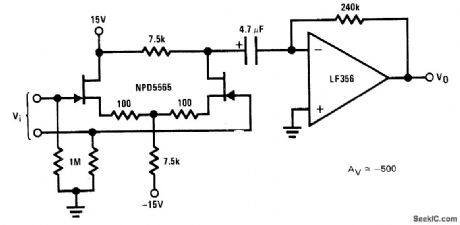
Differential connection of National NPD5565 dual JFET is used when balanced inputs and low distortion are main requirements for AC amplifier, Combination with LF356 opamp shown gives gain of about 500. Noise is somewhat higher than with single-ended JFET.- FET Databook, National Semiconductor, Santa Clara, CA, 1977, p 6-17-6-19. (View)
View full Circuit Diagram | Comments | Reading(1164)
POWER_BOOSTER_1
Published:2009/7/6 6:41:00 Author:May

Opamp power booster is used after conventional opamp when greater power-handling capability is required. 741 opamp circuit shown will drive moderate loads. Other opamps may be substituted in power stage if value of R1 is appropriately changed.- Signetics, Analog Data Manual, Signetics, Sunnyvale, CA, 1977, p 640-642. (View)
View full Circuit Diagram | Comments | Reading(2649)
JFET_INPUT
Published:2009/7/6 6:40:00 Author:May
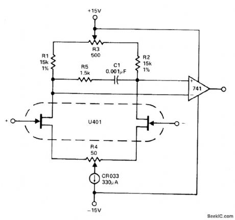
U401 dual JFET acting as preamp for standard bipolar opamp uses CR033 N-channel JFET as 330-pA current source. R4 is used to null initial offset. R3 is adjusted for minimum drift.- Analog Switches and Their Applications, Siliconix, Santa Clara, CA, 1976, p 7-51. (View)
View full Circuit Diagram | Comments | Reading(1958)
| Pages:1038/2234 At 2010211022102310241025102610271028102910301031103210331034103510361037103810391040Under 20 |
Circuit Categories
power supply circuit
Amplifier Circuit
Basic Circuit
LED and Light Circuit
Sensor Circuit
Signal Processing
Electrical Equipment Circuit
Control Circuit
Remote Control Circuit
A/D-D/A Converter Circuit
Audio Circuit
Measuring and Test Circuit
Communication Circuit
Computer-Related Circuit
555 Circuit
Automotive Circuit
Repairing Circuit