
Circuit Diagram
Index 1022
CD4047_CMOS_OSCILLATOR
Published:2009/7/22 2:21:00 Author:Jessie

This CMOS square-wave oscillator is based on the 4047 multivibrator circuit, which can be used for either monostable ( one-shot ) or astable applications. In the configuration shown, the 4047 is an astable multivibrator. There are three outputs from the 4047. The first is the oscillator (OSC) output, which is connected directly to the internal oscillator circuit. The other two outputs, Q and Q, are complementary to each other and operate at one half the frequency of the internal oscillator. The output frequency is set by timing components R1 and C1:
ƒo=1/(4.4R1C1)
R1 should be between 10,000 Ω and 1 MΩ, while C1 should be 100 pF or more (the maximum capacitance is not limited theoretically, but a practical limit exists when the leakage resistance of C1 is of the same order of magnitude as R1). (View)
View full Circuit Diagram | Comments | Reading(10142)
Compressor_expander_amplifiers
Published:2009/7/22 2:19:00 Author:Jessie

The maximum compression/expansion ratio of these circuits is set by the ratio of R1/R,as shown. (View)
View full Circuit Diagram | Comments | Reading(2476)
Low_impedance_microphone_Preamplifier
Published:2009/7/22 2:17:00 Author:Jessie
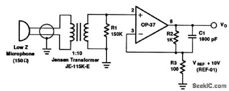
The low microphone impedance is matched to the OP-37 by thetransformer.C1 rolls off the high-frequency response at 90 kHz,giving a noise power bandwidth of 140 kHz. The REF-01 voltage reference is described In Fig.4-1. (View)
View full Circuit Diagram | Comments | Reading(0)
RC_OSCILLATOR
Published:2009/7/22 2:17:00 Author:Jessie

A single gate of a 4584 chip is connected in a simple RC square-wave audio-oscillator circuit. C1, R1, and R2 set the oscillator's frequency. The frequency range can be modified easily by changing the value of C1. The larger you make the capacitance, the lower the frequency range, and vice versa. Mylar, polystyrene, or a similar low-leakage capacitor works best in these high-impedance RC circuits. (View)
View full Circuit Diagram | Comments | Reading(1151)
Horn and Danger Signal Principle Diagram of Beijing CHEROKEE BJ2021 Light Off-road Vehicle
Published:2011/7/23 2:09:00 Author:Michel | Keyword: CHEROKEE, Light Off-road Vehicle, Horn, Danger Signal, Principle Diagram

Picture:Horn,Water Washing,Air Conditioning, Steering and Danger Signal Principle diagram of Beijing CHEROKEE BJ2021 Light Off-road Vehicle
l-buzzer,12-key switch,34-horn relay,35-horn button,36-electronic horn,44-compression hunger electromagnetic clutch,45-voltage switch,46-temperature switch,47-pour lamp,48-pour lamp switch,49-turn signal flasher unit,50-alarm flasher,51-steering and danger alertion switch,52-right steering signal light and steering indicator,53-left steering signal light and steering indicator 55-brake switch (View)
View full Circuit Diagram | Comments | Reading(770)
Low_noise_and_drift_FET_dc_amplifier
Published:2009/7/22 3:35:00 Author:Jessie

This circuit combines the low drift or a chopper-stabilized amplifier with a pair of FETs. As shown in Fig. 1-10B, the result is an amplifier with 0.05-μV/℃ drift, offset within 5 μV, 50-pA bias current, and 200-nV noise in a 0.1-to 10-Hz bandwidth. (View)
View full Circuit Diagram | Comments | Reading(1016)
Shift_right_shift_left_register_with_parallel_inputs
Published:2009/7/22 3:32:00 Author:Jessie
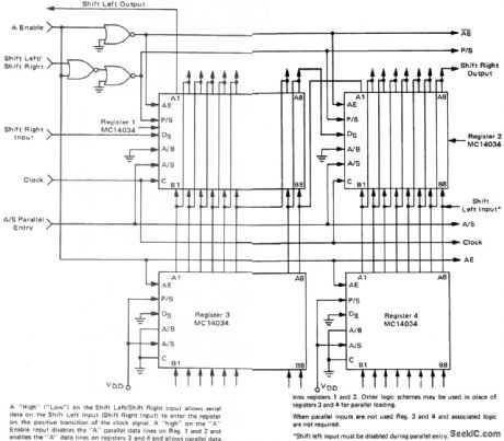
Shift-right/shift-left register with parallel inputs (courtesy Motorola Semiconductor Products Inc.). (View)
View full Circuit Diagram | Comments | Reading(1263)
Setting Timing Circuit of Power Supply Connection
Published:2011/7/26 0:54:00 Author:Michel | Keyword: Power Supply, Setting Timing Circuit

Picture 1 is setting timing circuit of power supply connection.When the power is connected,triggering PWL of ME555 feet 2 is below (1/3)Ucc and feet 3 outputs pulse during the time decided by R2 and C2.Then,+Ucc charges C2 via R2 and VD1 and charging voltage rises to +Ucc.Because of VD1 isolation function,R1 and C1 negative trigger the pulse.VD1 is fast charging diode when the power is off and it can keep the circuit working reliably when the circuit is off and turned on again and again in short time.NE55 outputs T high-level of pulse which is determined by R3 and C3,namely, T=R3C3.
Picture 1:Setting Timing Circuit of Power Supply Connection (View)
View full Circuit Diagram | Comments | Reading(828)
Low_noise_and_drift_dc_amplifier
Published:2009/7/22 3:32:00 Author:Jessie

This circuit combines the low noise of an LT1028 with a chopper-based carrier-modulation scheme to get a very low-noise, low-drift dc amplifier. As shown in Fig. 1-9B, noise in a 0.1- to 1-Hz bandwidth is less than 40 nV with 0.05 μV/℃ drift. In general, to maintain this low-noise performance, the source resistance should be kept below 500Ω. Such resistance is typical of transducers (strain-gauge bridges, magnetic detectors, etc.). (View)
View full Circuit Diagram | Comments | Reading(1554)
Temperature_senstive_heater_control
Published:2009/7/22 3:31:00 Author:Jessie
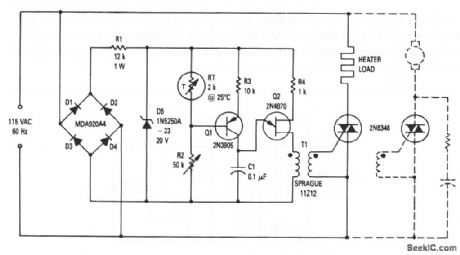
This circuit shows the basic UJT building block (Fig. 9-1) that is used to control an 800-W heater system. The simple RC circuit of Fig. 9-1 is replaced by Q1, RT and R2. Using phase control, the circuit is able to reduce power to the load as the desired temperature is reached, thus eliminating much of the overshoot inherent in mechanical controls. Although the circuit shown is for a heater, the circuit can also be used to control a constant-load motor (such as a blower motor), as indicated by the dotted portion of the diagram. The desired temperature is set by R2. The circuit can also be used for cooling by interchanging RT and R2. (View)
View full Circuit Diagram | Comments | Reading(2279)
Switchable_audio_amplifier
Published:2009/7/22 3:27:00 Author:Jessie

The SL6310 shown in this figure is a low-power audio amplifier that can be switched off by applying a mute signal to pins 7 or 8. Despite the low quiescent current consumption of 5 mA (only 0. 6 mA when muted), a minimum output power of400 mW is available into an 8-Ω load from a 9-V supply. With the values shown, the voltage gain is about 25, determined by the ratio of (R3+R4)/R3, with an input impedance of about 100KΩ), determined by,R1 and R2. (View)
View full Circuit Diagram | Comments | Reading(1027)
12_V_Battery_charger_control
Published:2009/7/22 3:27:00 Author:Jessie
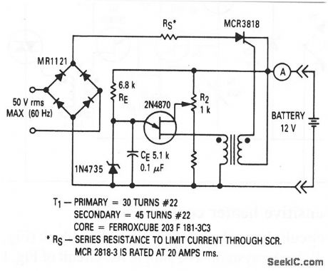
This circuit shows the basic UJT building block (Fig. 9-1) that is used to control a battery-charger system. Notice that the battery voltage controls the charger and, when the battery is fully charged, the charger will not supply current to the battery. The setting of R2 determines the amount of charge. Also, the charger will not work if battery polarity is reversed. (View)
View full Circuit Diagram | Comments | Reading(1)
Simple_time_delay
Published:2009/7/22 3:25:00 Author:Jessie
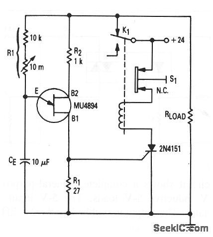
This circuit shows the basic UJT building block (Fig. 9-1) that is used to provide a simple time-delay function. When normally closed S1 is pushed, the SCR turns off, K1 is de-energized, and power is applied to the UJT relaxation oscillator and load. After a time delay that varys from less than 1 s to about 2.5 min.(as determined by the setting of the 1-MΩ pot), the UJT fires and turns on the SCR. K1 is energized and power is removed from the UJT and load. K1 stays energized until S1 is pushed again. (View)
View full Circuit Diagram | Comments | Reading(0)
Monolithic Stereo Play Intergrted Circuit
Published:2011/7/20 2:06:00 Author:Michel | Keyword: Monolithic, Stereo, Play Intergrted Circuit


LA4570 is cassette specific integrated circuit produced by SANYO Company.LA4570 are used in domestic, domestic assembly or import the monoplayer and cassette player.
First,LA4570 Inside Circuit Block Diagram and Pins FunctionsLA4570 integrated block is double preamplifying double power amplifier devices, with low voltage power supply and wide range, high gain, low consumption and less external components etc.advantages.One LA4570 and few external device can constitute monoplayer and cassette player.Its intergrated block inside circuit block diagram and typical application circuit are shown as picture 1.The IC adopts 16 feet DIP or flat package structure. The IC pins functions and data are shown as table 1.
Table 1: LA4570 IC Pins Functions and DataLA4570 Typical Application Circuit LA4570 typical application circuit of intergrated block is shown as picture 1. (View)
View full Circuit Diagram | Comments | Reading(2193)
Gain_controlled_microphone_preamplifier_VOGAD
Published:2009/7/22 3:25:00 Author:Jessie

The SL6270 shown in this figure combines the functions of audio amplifier and voice-operated gain-adjusting device (VOGAD). The SL6270 accepts signals from a low-sensitivitymicrophone and provides an essentially constant output signal for a 50-dB range of input. Thedynamic range, attack time, and decay time are controlled by external components. With thevalues shown. attack time(time taken for the output to return to within 10% of the original level following a 20-dB increase in input level)is about 20mS.decay rate is 20 dB/s .voltagegain is 52 dB with 72μVrms input at pin4,output level=90mVrms with 4mVrms input at pin4,and an input impedance of 150Ω. (View)
View full Circuit Diagram | Comments | Reading(3064)
Magnetic_cartridge_preamplifier
Published:2009/7/22 3:23:00 Author:Jessie

This circuit provides an approximate gain of 50 (34 dB) at 1 kHz with a distortion of 0.004%. If more gain is required, R3 can be decreased, but C3 must be increased proportionally to avoid loss of bias. C1, C2, R1, R2 provide RIAA equalization. C3 and R3 provide a rumble filter. The S/N ratio is better than 70 dB below a 5-mV input. (View)
View full Circuit Diagram | Comments | Reading(912)
High_wattage_lamp_control
Published:2009/7/22 3:21:00 Author:Jessie
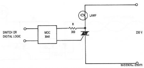
Many high-wattage incandescent lamps suffer shortened lifetimes when switched on at ac line voltages other than zero. This is because a large inrush of current destroys the filament. A simple solution to this problem is to use an optoisolator and triac, as shown. The triac must be capable of handling the lamp current. The MOC3041 optoisolator can be controlled from a switch or some form of 5-V digital logic. The minimum value of R is determined by the maximum surge current rating of the MOC3041 (ITSM), where: Rmin(pk) /ITSE; With a 230-V line, and a 1.2-A ITSM for the MOC3041, the minimum value of R is: 340 V/1.2A =283 Ω. (View)
View full Circuit Diagram | Comments | Reading(1254)
CMOS_256_word_by_n_bit_static_read_write_memory
Published:2009/7/22 3:19:00 Author:Jessie
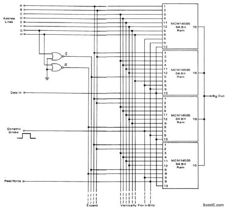
CMOS 256-word by n-bit static read/write memory (courtesy Motorola Semiconductor Products Inc.). (View)
View full Circuit Diagram | Comments | Reading(719)
Solid_state_relay
Published:2009/7/22 3:15:00 Author:Jessie
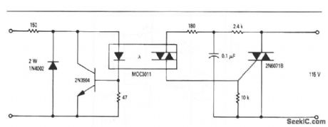
This circuit shows a complete, general-purpose, solid-state relay, snubbed for 115-V inductive 5-V loads. The 5-V input is protected by the MOC3011 optoisolator. The output is snubbed by the 2.4-kΩ resistor and 0.1-μF capacitor. (View)
View full Circuit Diagram | Comments | Reading(0)
TLC2932 Phase Locked Loop Clock Generating Integrated Circuit
Published:2011/7/20 1:34:00 Author:Michel | Keyword: Phase Locked, Loop Clock, Generating Integrated Circuit


TLC2932 is FLL clock generating IC produced by TEXAS.TLC2932 is mostly used in the DLP projection TV, in order to provide the clock signal for processing
circuits.TLC2932 integrated circuit contains the analog vco and phase detection circuit.Its inside circuit block diagram of intergrated block is shown as picture 1-1.
Picture 1-1:Inside Circuit Block Diagram of TLC2932 Intergrated Block
TL2932 adopts 14 feet DIP package and its pins functions and data are shown as table 1-2.
Table 1-2:Pins Functions and Data ofTLC2932 IC
(View)
View full Circuit Diagram | Comments | Reading(1132)
| Pages:1022/2234 At 2010211022102310241025102610271028102910301031103210331034103510361037103810391040Under 20 |
Circuit Categories
power supply circuit
Amplifier Circuit
Basic Circuit
LED and Light Circuit
Sensor Circuit
Signal Processing
Electrical Equipment Circuit
Control Circuit
Remote Control Circuit
A/D-D/A Converter Circuit
Audio Circuit
Measuring and Test Circuit
Communication Circuit
Computer-Related Circuit
555 Circuit
Automotive Circuit
Repairing Circuit