
Circuit Diagram
Index 1024
NE602_VARACTOR_TUNED_COLPITTS_VFO
Published:2009/7/22 3:53:00 Author:Jessie

You can use a varactor diode (D1) to tune a VFO circuit electronically. This figure shows a parallel-resonant, voltage-tuned Colpitts oscillator. (View)
View full Circuit Diagram | Comments | Reading(1067)
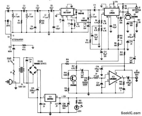
CARRIER_CURRENT_AM_RECEIVER
Published:2009/7/6 20:49:00 Author:May
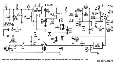
The AM Tuned Radio Frequency (TRF) receiver, has a sensitivity of about 1 mV at the input for an audio output of 1/2 W. Capacitor C22 couples audio signals from the power line to the PC board-it must be rated at 600 Vdc. R8 will cause Fl to blow, if C22 shorts. The signal from C22 goes to a tuned network (Ct through C5, L1, and L2) that has a 20-kHz bandwidth, which allows only the desired signal to pass through.
IC1 is again block i-f chip that has AGC capability and approximately 60 dB of gain. Components C8, C9, and L3, which are placed across the output of IC1, are broadly resonant around 280 kHz. C10 couples rf to detector-diode D1, which is used as an envelope detector.
The detector output is taken from C14,which sets the upper frequency limit at about 10 kHz or so.By reducing the value of C14, high frequency response can be obtatned. The detector output is connected to an external jack. Audio components are fed to audio-gain control R6, through C16 to IC2, an audio amplifier. C18 couples up to 1/2 watt of audio to an external speaker. The kit is available from North Country Radio, P.0. Box 53,Wykagyl Station, NY 10804. (View)
View full Circuit Diagram | Comments | Reading(1813)
Time_delay_with_constant_charging_current
Published:2009/7/22 3:51:00 Author:Jessie
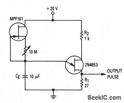
This circuit shows the basic UJT building block (Fig. 9-1), which is used to provide a time-delay function, where the charging current is constant and relatively small (less than 1 μA). This is done by replacing the basic RE, with a JFET and 10-MΩ pot. The 1-μA constant-charging current provides time delays up to about 10 min. (View)
View full Circuit Diagram | Comments | Reading(674)
SPEAKERPHONE
Published:2009/7/6 20:48:00 Author:May
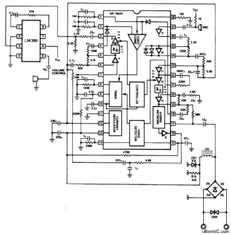
The XR-T6425 Speakerphone IC makes it possible to carry on conversation with-out using the handset, while the user is talking into a microphone and listening from a loudspeaker. It is ideal for hands-free conference calls. The XR-T6425 contains most of the circuits to eliminate singing and excessive background noise.
(View)
View full Circuit Diagram | Comments | Reading(2499)
01_1_100_and_1000_Hz_SINE_SQUARE_TRIANGLE_
Published:2009/7/6 20:47:00 Author:May

Provides choice of five spot frequencies switched in decades by S1. Setting of S2 determines shape of output waveform. Adjust R1, R2, and R3, to make peak-to-peak amplitudes of all three waveforms equal. R4, controls symmetry. R2 is adjusted for minimum distortion of sine-wave output. Output may be set up to 100 mA by R6, and is short-circuit-proof. DC level may be set anywhere between ±14 V by R7. Motorola 1438 IC and 741 opamp boost output of 8038 IC sufficiently to drive most laboratory loads.-G. R. Wilson, Low-requency Generator, Wireless World, Feb. 1977, p 44. (View)
View full Circuit Diagram | Comments | Reading(865)
VACKAR_VFO
Published:2009/7/22 3:50:00 Author:Jessie
This high-stability FET Vackar oscillator, covering 5.88 to 6.93 MHz, was developed by G3PDM in the late 1960s, but is still a valid design for HP VFOs for receiver, transmitter, and transceiver applications. (View)
View full Circuit Diagram | Comments | Reading(2836)
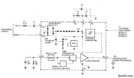
TONE_RINGER_Ⅱ
Published:2009/7/6 20:47:00 Author:May

The XR-T8205 Tone Ringer is primarily intended as a replacement for the mechanical telephone bell. The device can be powered directly from telephone ac ringing voltage or from a separate dc supply. An adjustable trigger level is provided with an external resistor. The circuit is designed for nominal 15 volt operation.
(View)
View full Circuit Diagram | Comments | Reading(1072)
Ratiometric_bridge_with_A_D_conversion
Published:2009/7/22 3:50:00 Author:Jessie

In this circuit, a MAX183 directly converts a bridge output to a 12-bit code using only two precision op amps. No differential-input instrumentation amplifier or reference is needed. The bottom of the bridge is driven by A1 so that the A1 inverting input remains at 0 V. The other bridge output is amplified by A2 in a basic noninverting configuration. No differential amplifier is needed because the bridge output to A2 is referenced to 0 V. The A1 output also drives the MAX183 VREF input so that reference changes (VDD is the reference) in the bridge excitation and the A/D track each other. (View)
View full Circuit Diagram | Comments | Reading(812)
VFO_TUNING_CIRCUITS
Published:2009/7/22 3:50:00 Author:Jessie

These are typical tuning circuits. The one in B is parallel resonant and the one in A is series resonant. (View)
View full Circuit Diagram | Comments | Reading(622)
CARRIER_CURRENT_FM_RECEIVER
Published:2009/7/6 20:45:00 Author:May
Input signals from the power line are coupled through C23 and R19 to the input filter network. C23 must be rated at 600 volts. Switch S2 is used as an attenuator. Components C2 through C7, L1 through L3, R1, and R20 form a triple-tuned bandpass filter having a passband from 220-340 kHz. Signals from the filter are fed to an MC1350P gain block IC, which is used as a tuned rf amplifier.
IC2, the LM565 PLL, is used as an FM demodulator. Pins 8 and 9 are connected to an internal VCO and components R9, R10, and C15 set the VCO's free running frequency. The VCO signal and the input signal from pin 2 are compared in the phase detector. The output from the phase detector is internally amplified, and then appears at pin 7. The output at pin 7 is a replica of the original modulation on the FM input signal to the receiver; the output at pin 7 is therefore the recovered audio. C17 and R14 couple audio to the base of Q2, which, in conjunction with R15, RIG, R17, and C18, form an audio amplifier that brings the recovered audio up to around 1 V peak-to-peak. The signal is then fed into an LM386N audio amplifier, which can deliver up to 1/2 W of audio, coupled via C20, to any standard 8- Ω external speaker. The kit is available from North Country Radio, P.O. Box 53, Wykagyl Station, NY 10804.
(View)
View full Circuit Diagram | Comments | Reading(2172)
TONE_RINGER
Published:2009/7/6 20:45:00 Author:May
The MC34012 tone-ringer chip derives its power by rectifying the ac ringing signal.That signal is normally at 20 Hz and measures between 70 and 130 volts rms. It uses that power for the tone generator and to drive the piezoelectric transducer. The sound that is produced is a warble that varies between two frequencies, f0/4 (f0 - 4) f0/5.The clock, or fundamental, frequency, f0, is generated by a relaxation oscillator. That oscillator has R2 and C2 as its frequency setting components providing a selectable range of 1 kHz to 10 kHz. Selecting different values for R2 and/or C2 changes the clock frequency, which in turn varies the warble frequencies. The MC34012 chip comes in three different warble rates at which the warble frequencies (f0/4, f0/5) are varied. These warble rates are f0/320, f0/640, or f0/160 and the different chips are designated as MC34012-1, -2, and -3, respectively. For example: with a 4.40 kHz oscillator frequency, the MC34012-1 produces 800 Hz and 1000 Hz tones with a 12.5 Hz warble rate. The MC34012-2 generates 1600 Hz and 2000 Hz tones with a similar 12.5 Hz warble frequency from an 8.0 kHz oscillator frequency. MC34012-3 will produce 400 Hz and 500 Hz tones with a 12.5 warble rate from a 2.0 kHz oscillator frequency. (View)
View full Circuit Diagram | Comments | Reading(896)
Manual_automatic_PROM_programmer
Published:2009/7/22 3:49:00 Author:Jessie
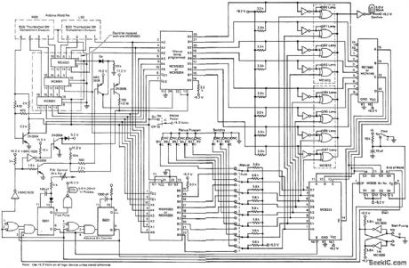
Manual/automatic PROM programmer (courtesy Motorola Semiconductor Products Inc.). (View)
View full Circuit Diagram | Comments | Reading(686)
POSITION_CONTROL_FOR_GRAPHICS
Published:2009/7/6 20:44:00 Author:May
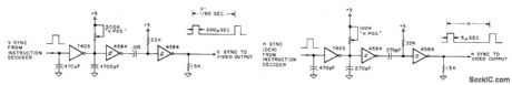
Six Inverters serve for moving entire character display to any position on TV screen,Display is produced by microprocessor through alphameric data-to-video converter. Circuit requires continuous feed of H and V signals from instruction decoder of microprocessor.-D. Lancaster, TVT Hardware Design, Kilobaud, Jan. 1978, p 64-68. (View)
View full Circuit Diagram | Comments | Reading(578)
NE602_VOLTAGE_TUNED_CLAPP_VFO
Published:2009/7/22 3:49:00 Author:Jessie

Here is a series-resonant, voltage-tuned Clapp oscillator circuit. (View)
View full Circuit Diagram | Comments | Reading(580)
TELEPHONE_IN_USEINDICATOR
Published:2009/7/6 20:42:00 Author:May
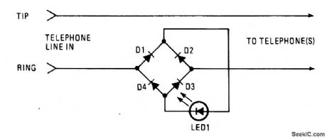
This circuit functions as a line-current sensor and can be connected in series with either of the phone lines. For the circuit to indicate an in use status for all phones on a single line, it must be connected in series with the phone line before, or ahead of all phones on the line. Since the power for the circuit is supplied by the phone company, a circuit could be added to each phone as an off-hook indicator. (View)
View full Circuit Diagram | Comments | Reading(510)
TELEPHONE_BLINKER
Published:2009/7/6 20:42:00 Author:May
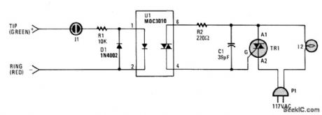
A small neon lamp is triggered into conduction by the telephone's ringing voltage, passes just enough current to activate the LED in optocoupler U1, which in tum triggers the 6-A Triac that controls I2-a 117-Vac lamp or bell. (Capacitor C1 is necessary only when the circuit is used to drive a bell.) The lamp will flash off-and-on at the ringing rate, which is normally around 20 Hz. If a 117 Vac bell is used, connect it in place of the lamp. (View)
View full Circuit Diagram | Comments | Reading(921)
SOFTWARE_MONITOR
Published:2009/7/6 20:40:00 Author:May

Detects large percent-age of random faults, such as overflow conditions. Based on fact that part of program passes through reentry on predictable repeat basis. For each reentry, pulse is fed from CPU to input of ,, 74LS123 retriggerable mono MVBR. On each pass through program, programmer sets and then resets MVBR. Period of mono is made longer than longest normal time between programmed pulse outputs, to prevent false alarms. Any system fault that makes program repeat instructions endlessly or lose control will give false indication.-D. Brickner, Get a Watch-dog to Monitor Those Real-Time Operations, Kilobaud, April 1978, p 118-119. (View)
View full Circuit Diagram | Comments | Reading(1206)
TIME_CONSTANT_DETECTOR_FOR_TV_CONTROL
Published:2009/7/23 1:33:00 Author:Jessie

Produces output pulse whose width is proportional to time constant of exponentially damped ultrasonic signal, in range of 0.1 to 0.5 sec, independent of input amplitude.-K. R. Cross and R. O. Whitaker, Time-Constant Detectors Control Tv Sets, Electronics, 32:36, p 62-67. (View)
View full Circuit Diagram | Comments | Reading(960)
ELECTRO_EXPLOSIVE_DEVICE_TESTER
Published:2009/7/23 1:32:00 Author:Jessie
Uses combination of tubes and solid-stctte thyrairon to generate single pulse up to 100 ump with duration of several millisec, for testing detonators, primers, squibs, and explosive switches.-V. W. Goldie, R. G. Amicone, and C. T. Davey, Generating Pulses With Solid. State Thyratrons, Electronics, 32;33, p 70. (View)
View full Circuit Diagram | Comments | Reading(811)
CARRIER_CURRENT_AUDIO_TRANSMITTER
Published:2009/7/6 20:40:00 Author:May

The decision to use either AM, narrowband FM (less than 15 kHz), or wideband FM (greater than 30 kHz) depends on the application. For the transmission of music, FM is better because it has greater noise immunity. For speech or other noncritical applications, AM may be satisfactory. Our transmitter permits either mode by switch selection.
Audio is fed from S1a to either the FM or AM circuitry. Starting with the FM section, amplifier Q1 accepts an audio signal in the 10 Hz to 20 kHz range of about 0.5 V peak-to-peak. The audio gain is adjusted via R5 to provide up to 60 kHz deviation of voltage-controlled oscillator IC1 which is set to nominally 280 kHz. IC1 and Q1 are supplied with a regulated 12 V from IC2. A square-wave signal from IC11pin 3 drives Q2, and Q2 drives the output amplifier Q3. A coupling network is used to match the nominal 45- Ω output impedance of Q3 to the 10- Ω ac line impedance.
In the AM mode, audio is coupled to Q8 via R24 and then amplified again by transistors Q4 to Q7. The normally stable dc voltage at test point A is thereby varied at an audio rate. Because Q2 and Q3 obtain their dc VCC from test point A, the VCO carrier input to Q2 is amplitude modulated by the varying VCC amplitude. That produces an amplitude-modulated output from the transmitter. Careful setting of carrier level R23 and audio level R24 provides up to 100% modulation. The kit is available from North Country Radio, P.O. Box 53, Wykagyl Station, NY 10804. (View)
View full Circuit Diagram | Comments | Reading(1262)
| Pages:1024/2234 At 2010211022102310241025102610271028102910301031103210331034103510361037103810391040Under 20 |
Circuit Categories
power supply circuit
Amplifier Circuit
Basic Circuit
LED and Light Circuit
Sensor Circuit
Signal Processing
Electrical Equipment Circuit
Control Circuit
Remote Control Circuit
A/D-D/A Converter Circuit
Audio Circuit
Measuring and Test Circuit
Communication Circuit
Computer-Related Circuit
555 Circuit
Automotive Circuit
Repairing Circuit