
Circuit Diagram
Index 1037
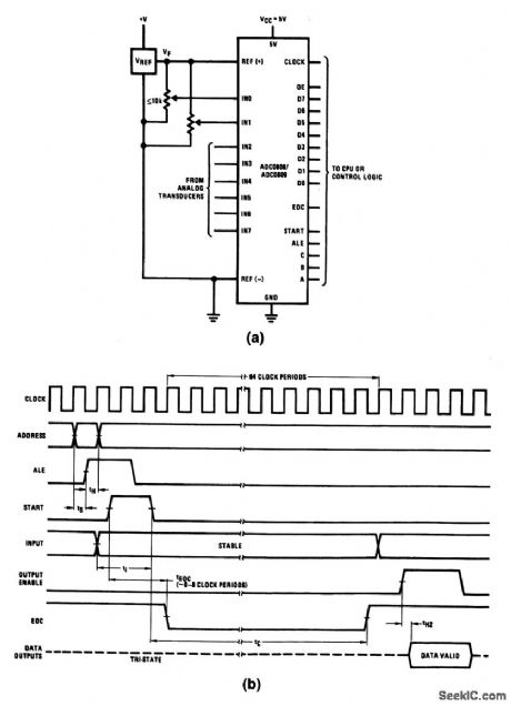
Ratiometric_A_D_converter_zoith_power_supply_reference
Published:2009/7/22 23:08:00 Author:Jessie
This circuit is similar to that of Fig. 6-13, except that the system power Supply is used as a reference. If used, supply noise must be kept to a minimum (with bypassing and separate supply-reference PC traces tapped as close as possible to the supply or regulator). (View)
View full Circuit Diagram | Comments | Reading(482)
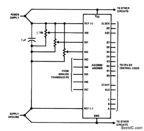
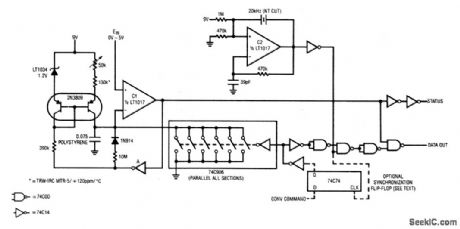
Ratiometric_A_D_converter_with_separate_reference
Published:2009/7/22 23:04:00 Author:Jessie

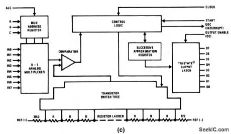

This circuit converts the output from eight ratiometric transducers to an 8-bit digital word using an ADC0808/0809 under control of a CPU or similar digital logic. Figure 6-13B shows the timing between the ADC and the CPU, while Fig. 6-13C shows the internal functions of the ADC. Notice that the ADC includes an SAR, as well as an 8-1 analog multiplexer. (View)
View full Circuit Diagram | Comments | Reading(1148)
FET_DRIVE
Published:2009/7/6 6:59:00 Author:May

National PF5102 JFET is combined with LF356 opamp to give low noise and high gain, for use as wide-bandwidth AC amplifier. Typical gain for combination shown is about 1000. Any other opamp can be used as long as it meets slew rate and bandwidth requirements.- FET Databook, National Semiconductor, Santa Clara, CA, 1977, p 6-17-6-19. (View)
View full Circuit Diagram | Comments | Reading(1099)
AUTOMATIC_BETA_CHECKER
Published:2009/7/22 23:02:00 Author:Jessie
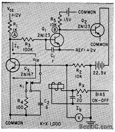
Holds collector current of test transistor Qx at preset value while base current is measured and bola de, termined.-E. P. Hojak, Automatic Measurement of Transistor Beta, Electronics, 32:49, p 114-115. (View)
View full Circuit Diagram | Comments | Reading(695)
TRAIN_CHUFFER
Published:2009/7/6 6:58:00 Author:May
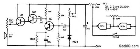
The circuit consists of a white nolse generator which only switches onwith the highpart of the square wave output from the clock circuit. The frequency of the clock ISadjusted with the 10 M pot and the output voltage of the clock IS adjusted by the 100k pot(rate and volume of chuff respectively).The 2M2 pot controls the amount of nolseproduced and the 1 k pot on the speaker controls the pitch of the average nolse. (View)
View full Circuit Diagram | Comments | Reading(687)
CMOS_A_D_converter_with_serial_output
Published:2009/7/22 22:56:00 Author:Jessie
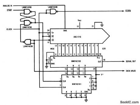
In this circuit, 12 bits of data are shifted out serially using an MM74C150. This permits valid data to be available at the serial output port as fast as half a clock cycle after the most current decision. The data bits are synchronized to the falling edge of the system clock. (View)
View full Circuit Diagram | Comments | Reading(689)
1_A_CURRENT_BOOSTER
Published:2009/7/6 6:58:00 Author:May
Used with LM143 high-voltage opamp to increase output current while providing short-circuit protection and low crossover distortion. With 40-ohm load, output voltage can swing to + 29.6 V and -28 V. All four transistors should be on Thermalloy 6006B or equivalent common heatsink. All diodes are 1N3193.- Linear Applications, Vol. 2, National Semiconductor, Santa Clara, CA, 1976, AN-127, p 4-5. (View)
View full Circuit Diagram | Comments | Reading(915)
Video_system_channel_control_box
Published:2009/7/22 22:39:00 Author:Jessie
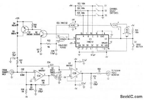
In the channel control box of the single-coax video system (Fig. 3-14), a desired channel is encoded by three bits, set either by switches (as shown) or by an applied digital input. Momentary depression of the send button triggers down-converter IC1 and gated oscillator IC2A to initiate a channel-selection burst.Supply current flows to the remote multiplexor box through Q1 (normally on and saturated), R27, and the coax center conductor. R27 also terminates the coax via C21. When Q1 turns off momentarily, forward bias across D3 and D4 develops a negative 1.2-V channel-select pulse. This 1.2-V drop in supply voltage does not affect the remote multiplexer video output. Consequently, the video monitor display does not flip during channel changes, provided that the channel signals have common sync timing. The short time constant that is associated with coupling of video to the coax (C11 and R9, R27) enables selection of any channel in less than one second, but also allows the video sync-pulse baseline to shift with picture content. To prevent this shift, peak detector IC3A drives Q3, which applies dc restoration ahead of IC3B. During each negative sync pulse, Q3 turns on just long enough to reclamp the pulse tip at 0 V. (View)
View full Circuit Diagram | Comments | Reading(1008)
ELECTRONICS_BONGOS
Published:2009/7/6 6:57:00 Author:May


This circuit consists of twin-T sine-wave oscillators. Each oscillator has a filter in the feedback loop. If the loop gain is greater than unity, the circuit will oscillate. Gain is adjusted to be just less than unity. Touching the touch plate starts the oscillator, but the moment your finger is removed from the touch plate the oscillations will die away.The rate of decay is a function of circuit gain and controlled by RV1 (and RV3). (View)
View full Circuit Diagram | Comments | Reading(667)
LOW_NOISE_5_kHz
Published:2009/7/6 6:56:00 Author:May
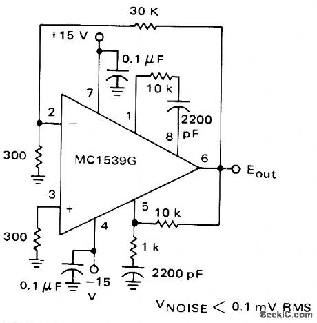
Values shown are for operation of Motorola MC1539G opamp in closed-loop mode with noninverting gain of 100 and source impedance of about 300 ohms. Circuit bandwidth is about 5 kHz.-E. Renschler, The MC1539 Operational Amplifier and Its Applications, Motorola, Phoenix, AZ, 1974, AN-439, p 19. (View)
View full Circuit Diagram | Comments | Reading(549)
GAIN_CONTROLLED_AMPLIFIER
Published:2009/7/6 6:55:00 Author:May
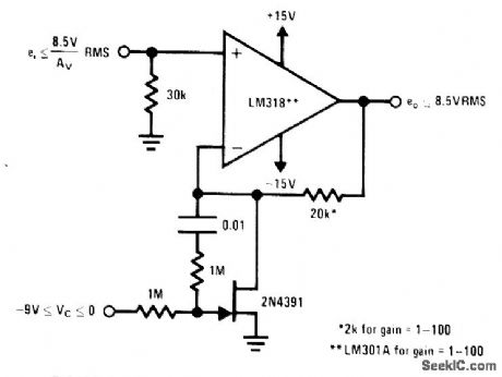
Control voltage in range of 0 to -9 V provides gain range of 1 to 1000 for National LM318 opamp using FET in feedback path. Bandwidth is better than 20 kHz at maximum gain. Applications include remote or multichannel gain control, volume expansion, and volume compression/limiting.-J. Sherwin, A Linear Multiple Gain-Controlled Amplifier, National Semiconductor, Santa Clara, CA, 1975, AN-129, p 5. (View)
View full Circuit Diagram | Comments | Reading(3741)
60_kHz_PRECISION_RECTIFIER
Published:2009/7/6 6:54:00 Author:May
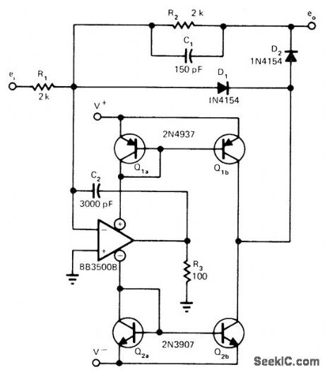
Usable full-power response of typical opamp is boosted to 60 kHz while giving 300-kHz small-signal band width. Circuit uses transistors to provide speed boosting gain during transition from one precision rectifier diode to the other in feedback loop of opamp. Added stage is driven from power-supply current drains of opamp. Article traces operation of circuit in detail-J. Graeme, Boost Precision Rectifier BW above That of Op Amp Used, EDN Magazine, July 5, 1974, p 67-69. (View)
View full Circuit Diagram | Comments | Reading(695)
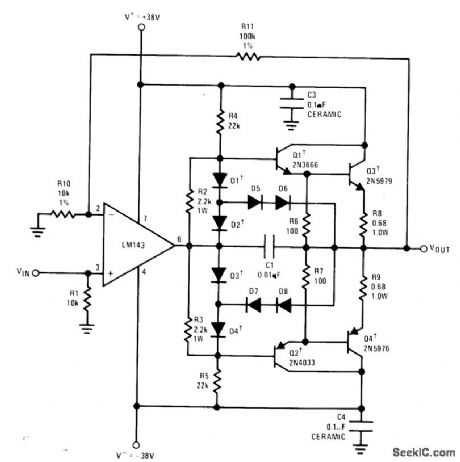
8_A_CURRENT_BOOSTER
Published:2009/7/6 6:53:00 Author:May
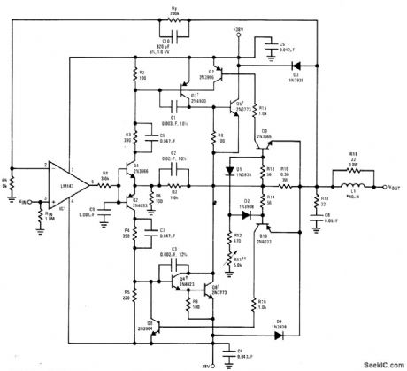
High-compliance power stage for LM143 high-voltage opamp provides very high peak drive currents along with output voltage swings to within 4 V of ±38 V supply under full load. Maximum output current depends on setting of current-adjusting pot R11 and on output voltage. Limit ranges from 14 A when R11 is 0 down to about 4 A for 5K. Maximum power output is 144 WRMS, for which frequency response is 3 dB down at 10 kHz. Voltage gain is 21. Q3-Q6 should be on common Thermalloy 6006B or equivalent heat-sink,- Linear Applications, Vol. 2, National Semiconductor, Santa Clara, CA, 1976, AN-127, p 5-6. (View)
View full Circuit Diagram | Comments | Reading(3023)
Low_power_10_bit_A_D_converter_1
Published:2009/7/22 22:31:00 Author:Jessie
This circuit is similar to that of Fig. 6-6, except that no external clock is required and typical quiescent power consumption is about 100 μA. Also, the additional ±1 LSB uncertainty of the Fig. 6-6 circuit is eliminated when the flip-flop shown in dashed lines is used. To calibrate, adjust the 50-kΩ pot for 1024 counts with 5.000 V at the input. (View)
View full Circuit Diagram | Comments | Reading(472)
SINGLE_SUPPLY_POSTAMPLIFIER
Published:2009/7/6 6:51:00 Author:May
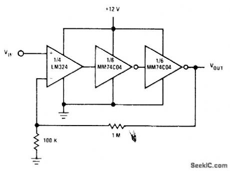
Use of two sections of MM74C04 as postamolifier for LM324 single-supply amplifier gives open-loop gain of about 160 dB Additional CMOS inverter sections can be paralleled for increased power to drive higher current loads; each MM74C04 section is rated for 5-mA load.- Linear Application, Vol. 2, National Semiconductor, Santa Clara, CA, 1976, AN-88, p 2. (View)
View full Circuit Diagram | Comments | Reading(679)
Video_amplifier_dc_stabilizer_differential_inputs
Published:2009/7/22 22:29:00 Author:Jessie
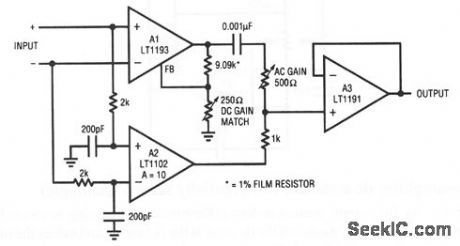
This circuit shows a way to get full differential inputs with dc-stabilized operation. A1 and A2 both (differentially) sense the input at gains of 10. The A3 output is an undistorted, amplified version (in this case, time 10) of the input. The circuit is adjusted by applying a square wave and adjusting the ac gain for the squarest comers, and the dc gain-match for a flat top. Circuit bandwidth exceeds 35 MHz, slew rate is 450 V/μs, and dc offset is about 200μV. (View)
View full Circuit Diagram | Comments | Reading(628)
Fast_optically_isolated_transistor_or_switch
Published:2009/7/22 22:28:00 Author:Jessie
This circuit is similar to that of Fig. 9-54, but it has better ac response. The cathode of D2 is returned to a separate positive supply, rather than to the collector of Q1, which eliminates the added collector-to-base capacitance of D2. With this circuit, a 40-V 1-A load can be switched in 500 ns. Any photosensitive diode can be used for D2, instead of the optoisolator, to make a light-activated switch. (View)
View full Circuit Diagram | Comments | Reading(825)
Video_amplifier_dc_stabilizer_servo_controlled_FET
Published:2009/7/22 22:27:00 Author:Jessie
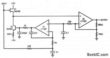
This circuit is a wideband, highly stable, gain-of-10amplifier with high input impedance. Input capacitance is about 3 pF. A2 provides a 100-MHz bandwidth gain of 10 (using the values shown). With an input capacitance of 3 pF and bias current of 100 pA, the circuit is well suited to a variety of video applications. (View)
View full Circuit Diagram | Comments | Reading(764)
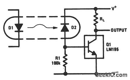
Optically_isolated_power_transistor
Published:2009/7/22 22:26:00 Author:Jessie
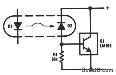
In this circuit, D1 and D2 can be part of almost any standard optocoupler or optoisolator. With no drive, R1 absorbs the base current of Q1, holding Q1 off. When power is applied to D1 (or to the LED of an optocoupler), D2 allows current to flow from the collector to base. Less than 20 μA is required from D2 to turn the LM1195 fully on。 (View)
View full Circuit Diagram | Comments | Reading(596)
Optocoupler_that_is_used_as_a_pulse_amplifier
Published:2009/7/22 22:23:00 Author:Jessie
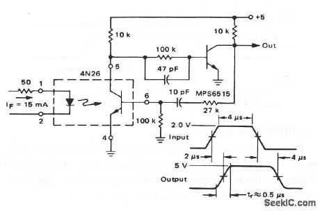
This circuit shows a 4N26 combined with a transistor to form a simple pulse amplifier that uses positive feedback to the 4N26 base. The feedback decreases pulse rise time from about 2 to 0.5 μs. (View)
View full Circuit Diagram | Comments | Reading(758)
| Pages:1037/2234 At 2010211022102310241025102610271028102910301031103210331034103510361037103810391040Under 20 |
Circuit Categories
power supply circuit
Amplifier Circuit
Basic Circuit
LED and Light Circuit
Sensor Circuit
Signal Processing
Electrical Equipment Circuit
Control Circuit
Remote Control Circuit
A/D-D/A Converter Circuit
Audio Circuit
Measuring and Test Circuit
Communication Circuit
Computer-Related Circuit
555 Circuit
Automotive Circuit
Repairing Circuit